- 您現(xiàn)在的位置:買賣IC網(wǎng) > PDF目錄45359 > MPC8306VMABDCA (FREESCALE SEMICONDUCTOR INC) 32-BIT, 133 MHz, RISC PROCESSOR, PBGA369 PDF資料下載
參數(shù)資料
| 型號(hào): | MPC8306VMABDCA |
| 廠商: | FREESCALE SEMICONDUCTOR INC |
| 元件分類: | 微控制器/微處理器 |
| 英文描述: | 32-BIT, 133 MHz, RISC PROCESSOR, PBGA369 |
| 封裝: | 19 X 19 MM, 1.61 MM HEIGHT, 0.80 MM PITCH, LEAD FREE, MAPBGA-369 |
| 文件頁(yè)數(shù): | 26/76頁(yè) |
| 文件大小: | 474K |
| 代理商: | MPC8306VMABDCA |
第1頁(yè)第2頁(yè)第3頁(yè)第4頁(yè)第5頁(yè)第6頁(yè)第7頁(yè)第8頁(yè)第9頁(yè)第10頁(yè)第11頁(yè)第12頁(yè)第13頁(yè)第14頁(yè)第15頁(yè)第16頁(yè)第17頁(yè)第18頁(yè)第19頁(yè)第20頁(yè)第21頁(yè)第22頁(yè)第23頁(yè)第24頁(yè)第25頁(yè)當(dāng)前第26頁(yè)第27頁(yè)第28頁(yè)第29頁(yè)第30頁(yè)第31頁(yè)第32頁(yè)第33頁(yè)第34頁(yè)第35頁(yè)第36頁(yè)第37頁(yè)第38頁(yè)第39頁(yè)第40頁(yè)第41頁(yè)第42頁(yè)第43頁(yè)第44頁(yè)第45頁(yè)第46頁(yè)第47頁(yè)第48頁(yè)第49頁(yè)第50頁(yè)第51頁(yè)第52頁(yè)第53頁(yè)第54頁(yè)第55頁(yè)第56頁(yè)第57頁(yè)第58頁(yè)第59頁(yè)第60頁(yè)第61頁(yè)第62頁(yè)第63頁(yè)第64頁(yè)第65頁(yè)第66頁(yè)第67頁(yè)第68頁(yè)第69頁(yè)第70頁(yè)第71頁(yè)第72頁(yè)第73頁(yè)第74頁(yè)第75頁(yè)第76頁(yè)
MPC8306 PowerQUICC II Pro Integrated Communications Processor Family Hardware Specifications, Rev. 0
32
Freescale Semiconductor
HDLC
reference the rising edge of the clock, these AC timing diagrams also apply when the falling edge is the
active edge.
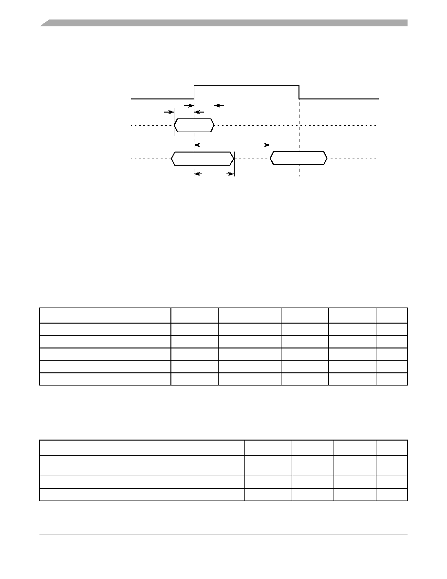
Figure 21. TDM/SI AC Timing (External Clock) Diagram
10 HDLC
This section describes the DC and AC electrical specifications for the high level data link control (HDLC),
of the MPC8306.
10.1
HDLC DC Electrical Characteristics
Table 30 provides the DC electrical characteristics for the MPC8306 HDLC protocol.
10.2
HDLC AC Timing Specifications
Table 31 provides the input and output AC timing specifications for HDLC protocol.
Table 30. HDLC DC Electrical Characteristics
Characteristic
Symbol
Condition
Min
Max
Unit
Output high voltage
VOH
IOH = –2.0 mA
2.4
—
V
Output low voltage
VOL
IOL = 3.2 mA
—
0.5
V
Input high voltage
VIH
—2.0
OVDD +0.3
V
Input low voltage
VIL
—–0.3
0.8
V
Input current
IIN
0 V
VIN OVDD
—
±5
A
Table 31. HDLC AC Timing Specifications1
Characteristic
Symbol2
Min
Max
Unit
Outputs—Internal clock delay
tHIKHOV
09
ns
Outputs—External clock delay
tHEKHOV
1
12
ns
Outputs—Internal clock high impedance
tHIKHOX
05.5
ns
TDM/SICLK (Input)
tSEIXKH
tSEIVKH
tSEKHOV
Input Signals:
TDM/SI
(See Note)
Output Signals:
TDM/SI
(See Note)
Note:
The clock edge is selectable on TDM/SI.
tSEKHOX
相關(guān)PDF資料 |
PDF描述 |
|---|---|
| MPC8306CVMADDCA | 32-BIT, 266 MHz, RISC PROCESSOR, PBGA369 |
| MPC8308CZQAGD | 32-BIT, 266 MHz, MICROPROCESSOR, PBGA473 |
| MPC8308CZQADD | 32-BIT, 266 MHz, MICROPROCESSOR, PBGA473 |
| MPC8308CVMAFD | 32-BIT, 266 MHz, MICROPROCESSOR, PBGA473 |
| MPC8309CVMAGDCA | 32-BIT, 400 MHz, RISC PROCESSOR, PBGA489 |
相關(guān)代理商/技術(shù)參數(shù) |
參數(shù)描述 |
|---|---|
| MPC8306VMACDC | 制造商:Freescale Semiconductor 功能描述:MPC8306VMACDC - Bulk |
| MPC8306VMACDCA | 功能描述:微處理器 - MPU E300 MP 200 RoHS:否 制造商:Atmel 處理器系列:SAMA5D31 核心:ARM Cortex A5 數(shù)據(jù)總線寬度:32 bit 最大時(shí)鐘頻率:536 MHz 程序存儲(chǔ)器大小:32 KB 數(shù)據(jù) RAM 大小:128 KB 接口類型:CAN, Ethernet, LIN, SPI,TWI, UART, USB 工作電源電壓:1.8 V to 3.3 V 最大工作溫度:+ 85 C 安裝風(fēng)格:SMD/SMT 封裝 / 箱體:FBGA-324 |
| MPC8306VMADDC | 制造商:Freescale Semiconductor 功能描述:MPC8306VMADDC - Bulk |
| MPC8306VMADDCA | 功能描述:微處理器 - MPU E300 MP 266 RoHS:否 制造商:Atmel 處理器系列:SAMA5D31 核心:ARM Cortex A5 數(shù)據(jù)總線寬度:32 bit 最大時(shí)鐘頻率:536 MHz 程序存儲(chǔ)器大小:32 KB 數(shù)據(jù) RAM 大小:128 KB 接口類型:CAN, Ethernet, LIN, SPI,TWI, UART, USB 工作電源電壓:1.8 V to 3.3 V 最大工作溫度:+ 85 C 安裝風(fēng)格:SMD/SMT 封裝 / 箱體:FBGA-324 |
| MPC8306VMADDCA | 制造商:Freescale Semiconductor 功能描述:IC 32-BIT MPU 266 MHz 369-LFBGA |
發(fā)布緊急采購(gòu),3分鐘左右您將得到回復(fù)。