- 您現(xiàn)在的位置:買賣IC網(wǎng) > PDF目錄45328 > MK2049-11SITRLF 56 MHz, OTHER CLOCK GENERATOR, PDSO20 PDF資料下載
參數(shù)資料
| 型號: | MK2049-11SITRLF |
| 元件分類: | 時(shí)鐘產(chǎn)生/分配 |
| 英文描述: | 56 MHz, OTHER CLOCK GENERATOR, PDSO20 |
| 封裝: | 0.300 INCH, SOIC-20 |
| 文件頁數(shù): | 11/13頁 |
| 文件大小: | 166K |
| 代理商: | MK2049-11SITRLF |

Communications Clock PLL
MDS 2049-11 C
7
Revision 021402
Integrated Circuit Systems, Inc. q 525 Race Street San Jose, CA 95126 q tel (408) 295-9800 q
www.icst.com
MK2049-11
capacitor should be a tantalum type, 1
F minimum.
The other capacitors should be ceramic type.
The power supply traces to the individual VDD pins
should fan out at the common supply filter to reduce
interaction between the device circuit blocks.
The decoupling capacitors at the VDD pins should be
ceramic type and should be as close to the VDD pin
as possible. There should be no via’s between the
decoupling capacitor and the supply pin.
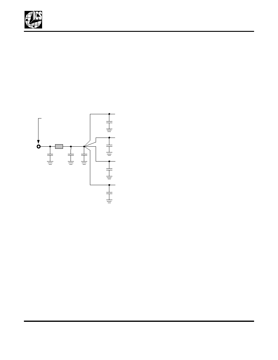
Recommended Power Supply Connection
Series Termination Resistor
Output clock PCB traces over 1 inch should use series
termination to maintain clock signal integrity and to
reduce EMI. To series terminate a 50
trace, which is a
commonly used PCB trace impedance, place a 33
resistor in series with the clock line as close to the clock
output pin as possible. The nominal impedance of the
clock output is 20
.
Quartz Crystal
The MK2049-11 operates by phase-locking the VCXO
circuit to the input signal at the ICLK input. The VCXO
consists of the external crystal and the integrated
VCXO oscillator circuit. To achieve the best
performance and reliability, a crystal device with the
recommended parameters (shown below) must be
used, and the layout guidelines discussed in the
following section shown must be followed.
The frequency of oscillation of a quartz crystal is
determined by its cut and by the load capacitors
connected to it. The MK2049-11 incorporates variable
load capacitors on-chip which “pull” or change the
frequency of the crystal. The crystals specified for use
with the MK2049-11 are designed to have zero
frequency error when the total of on-chip + stray
capacitance is 14pF. To achieve this, the layout should
use short traces between the MK2049-11 and the
crystal.
Recommended Crystal Parameters:
Operating Temperature Range
Commercial Applications
0 to 70
°C
Industrial Applications
-40 to 85
°C
Initial Accuracy at 25
°C
±20 ppm
Temperature Stability
±30 ppm
Aging
±20 ppm
Load Capacitance
14 pF
Shunt Capacitance, C0
7 pF Max
C0/C1 Ratio
250 Max
Equivalent Series Resistance
35
Max
Note: Crystals used in production should be screened
for 3rd overtone modes and spurs over the range of (3x
crystal frequency) +/- 100ppm, when measured at the
nominal parallel resonant frequency. Failure to do so
may cause locking problems in a small percentage of
production systems at certain input frequencies.
Crystal Tuning Load Capacitors
The crystal traces should include pads for small
capacitors from X1 and X2 to ground, shown as CL in
the Block Diagram on page 1. These capacitors are
optional and may be later used to center the total load
capacitor adjustment range imposed on the crystal.
The load adjustment range includes stray PCB
capacitance that varies with board layout. Because the
typical telecom reference frequency is accurate to less
Connection Via to
5V Power Plane
Ferrite
Chip
0.
1
F
BULK
1
n
F
VDD
Pin
0.0
1
F
VDD
Pin
0.
01
F
VDD
Pin
0.
0
1
F
VDD
Pin
0.
01
F
相關(guān)PDF資料 |
PDF描述 |
|---|---|
| MK2049-11SITRLF | 56 MHz, OTHER CLOCK GENERATOR, PDSO20 |
| MK2049-11SI | 56 MHz, OTHER CLOCK GENERATOR, PDSO20 |
| MK2049-45ASI | 125 MHz, OTHER CLOCK GENERATOR, PDSO20 |
| MK2069-01GILFTR | 160 MHz, OTHER CLOCK GENERATOR, PDSO56 |
| MK2069-01GITR | 160 MHz, OTHER CLOCK GENERATOR, PDSO56 |
相關(guān)代理商/技術(shù)參數(shù) |
參數(shù)描述 |
|---|---|
| MK2049-34 | 制造商:ICS 制造商全稱:ICS 功能描述:3.3 V Communications Clock PLL |
| MK2049-34A | 制造商:ICS 制造商全稱:ICS 功能描述:3.3 Volt Communications Clock VCXO PLL |
| MK2049-34SAI | 功能描述:IC VCXO PLL CLK SYNTH 20-SOIC RoHS:否 類別:集成電路 (IC) >> 時(shí)鐘/計(jì)時(shí) - 時(shí)鐘發(fā)生器,PLL,頻率合成器 系列:- 標(biāo)準(zhǔn)包裝:39 系列:- 類型:* PLL:帶旁路 輸入:時(shí)鐘 輸出:時(shí)鐘 電路數(shù):1 比率 - 輸入:輸出:1:10 差分 - 輸入:輸出:是/是 頻率 - 最大:170MHz 除法器/乘法器:無/無 電源電壓:2.375 V ~ 3.465 V 工作溫度:0°C ~ 70°C 安裝類型:* 封裝/外殼:* 供應(yīng)商設(shè)備封裝:* 包裝:* |
| MK2049-34SAILF | 功能描述:時(shí)鐘合成器/抖動清除器 3.3 VOLT COMMUNICA. CLOCK VCXO PLL RoHS:否 制造商:Skyworks Solutions, Inc. 輸出端數(shù)量: 輸出電平: 最大輸出頻率: 輸入電平: 最大輸入頻率:6.1 GHz 電源電壓-最大:3.3 V 電源電壓-最小:2.7 V 封裝 / 箱體:TSSOP-28 封裝:Reel |
| MK2049-34SAILFTR | 功能描述:時(shí)鐘合成器/抖動清除器 3.3 VOLT COMMUNICA. CLOCK VCXO PLL RoHS:否 制造商:Skyworks Solutions, Inc. 輸出端數(shù)量: 輸出電平: 最大輸出頻率: 輸入電平: 最大輸入頻率:6.1 GHz 電源電壓-最大:3.3 V 電源電壓-最小:2.7 V 封裝 / 箱體:TSSOP-28 封裝:Reel |
發(fā)布緊急采購,3分鐘左右您將得到回復(fù)。