- 您現(xiàn)在的位置:買賣IC網(wǎng) > PDF目錄378672 > MJW16206 (ON SEMICONDUCTOR) POWER TRANSISTORS PDF資料下載
參數(shù)資料
| 型號(hào): | MJW16206 |
| 廠商: | ON SEMICONDUCTOR |
| 元件分類: | 功率晶體管 |
| 英文描述: | POWER TRANSISTORS |
| 中文描述: | 12 A, 500 V, NPN, Si, POWER TRANSISTOR, TO-247AE |
| 封裝: | CASE 340K-01, 3 PIN |
| 文件頁數(shù): | 6/10頁 |
| 文件大小: | 342K |
| 代理商: | MJW16206 |
6
Motorola Bipolar Power Transistor Device Data
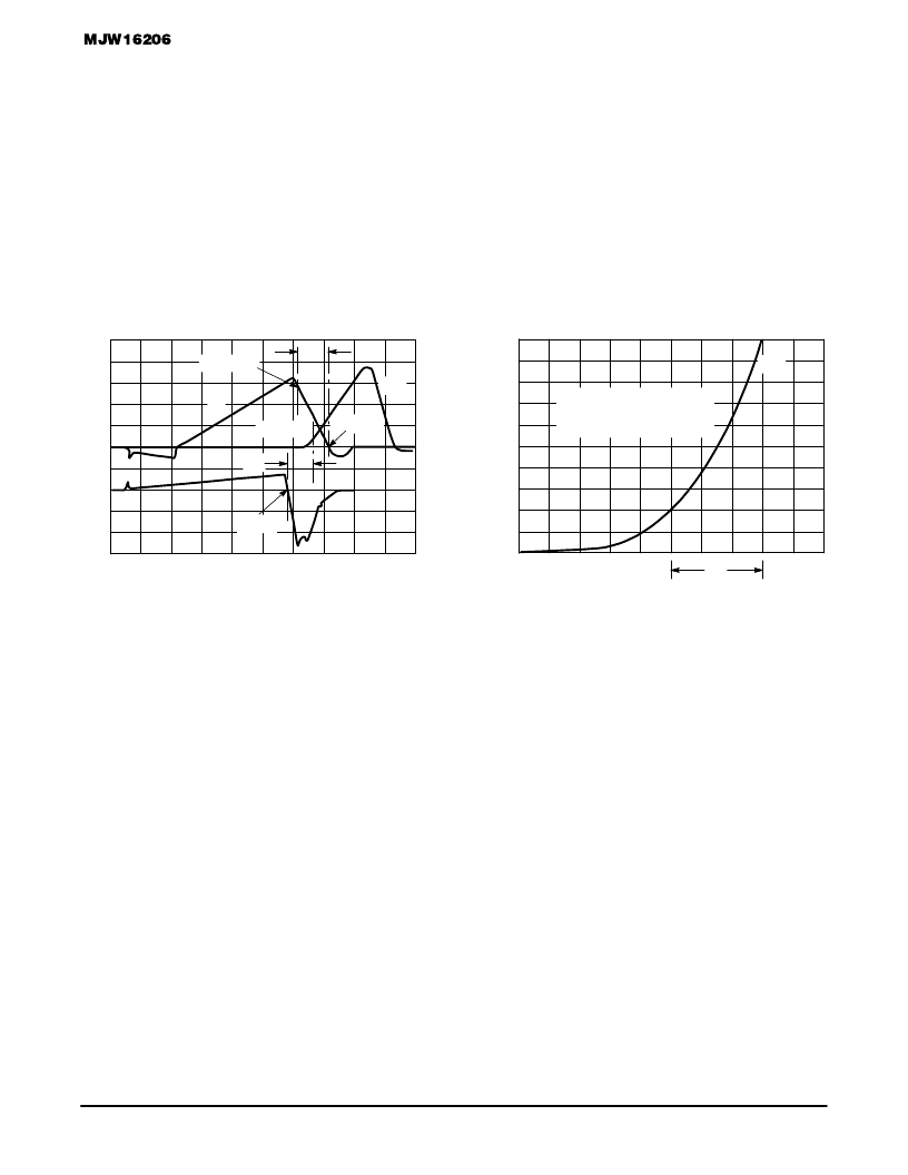
DYNAMIC DESATURATION
DYNAMIC DESATURATION
The SCANSWITCH series of bipolar power transistors are
specifically designed to meet the unique requirements of hor-
izontal deflection circuits in computer monitor applications.
Historically, deflection transistor design was focused on mini-
mizing collector current fall time. While fall time is a valid
figure of merit, a more important indicator of circuit perfor-
mance as scan rates are increased is a new characteristic,
“dynamic desaturation.” In order to assure a linear collector
current ramp, the output transistor must remain in hard satu-
ration during storage time and exhibit a rapid turn–off transi-
tion. A sluggish transition results in serious consequences.
As the saturation voltage of the output transistor increases,
the voltage across the yoke drops. Roll off in the collector
current ramp results in improper beam deflection and distor-
tion of the image at the right edge of the screen. Design
changes have been made in the structure of the SCANS-
WITCH series of devices which minimize the dynamic desa-
turation interval. Dynamic desaturation has been defined in
terms of the time required for the VCE to rise from 1.0 to
5.0 volts (Figures 13 and 14) and typical performance at opti-
mized drive conditions has been specified. Optimization of
device structure results in a linear collector Current ramp, ex-
cellent turn–off switching performance, and significantly low-
er overall power dissipation.
Figure 13. Deflection Simulator Switching
Waveforms From Circuit in Figure 15
IC
0% IB
VCE
tsv
VCE = 20 V
tfi
10% IC(pk)
Figure 14. Definition of Dynamic
Desaturation Measurement
TIME (ns)
VCE
DYNAMIC DESATURATION TIME
IS MEASURED FROM VCE = 1 V
TO VCE = 5 V
tds
1
4
C
5
0
3
2
0
0
90% IC(pk)
相關(guān)PDF資料 |
PDF描述 |
|---|---|
| MJW16212 | POWER TRANSISTOR 10 AMPERES 1500 VOLTS - VCES 50 AND 150 WATTS |
| MJW16212 | POWER TRANSISTOR |
| MJW21191 | 8.0 AMPERES POWER TRANSISTORS COMPLEMENTARY SILICON 150 VOLTS 100 WATTS |
| MJW21191 | POWER TRANSISTORS COMPLEMENTARY SILICON |
| MJW21192 | POWER TRANSISTORS COMPLEMENTARY SILICON |
相關(guān)代理商/技術(shù)參數(shù) |
參數(shù)描述 |
|---|---|
| MJW16212 | 制造商:Rochester Electronics LLC 功能描述:- Bulk |
| MJW18020 | 功能描述:兩極晶體管 - BJT 20A 450V 250W NPN RoHS:否 制造商:STMicroelectronics 配置: 晶體管極性:PNP 集電極—基極電壓 VCBO: 集電極—發(fā)射極最大電壓 VCEO:- 40 V 發(fā)射極 - 基極電壓 VEBO:- 6 V 集電極—射極飽和電壓: 最大直流電集電極電流: 增益帶寬產(chǎn)品fT: 直流集電極/Base Gain hfe Min:100 A 最大工作溫度: 安裝風(fēng)格:SMD/SMT 封裝 / 箱體:PowerFLAT 2 x 2 |
| MJW18020_10 | 制造商:ONSEMI 制造商全稱:ON Semiconductor 功能描述:NPN Silicon Power Transistors High Voltage Planar |
| MJW18020G | 功能描述:兩極晶體管 - BJT 20A 450V 250W NPN RoHS:否 制造商:STMicroelectronics 配置: 晶體管極性:PNP 集電極—基極電壓 VCBO: 集電極—發(fā)射極最大電壓 VCEO:- 40 V 發(fā)射極 - 基極電壓 VEBO:- 6 V 集電極—射極飽和電壓: 最大直流電集電極電流: 增益帶寬產(chǎn)品fT: 直流集電極/Base Gain hfe Min:100 A 最大工作溫度: 安裝風(fēng)格:SMD/SMT 封裝 / 箱體:PowerFLAT 2 x 2 |
| MJW21191 | 功能描述:兩極晶體管 - BJT 8A 150V 100W PNP RoHS:否 制造商:STMicroelectronics 配置: 晶體管極性:PNP 集電極—基極電壓 VCBO: 集電極—發(fā)射極最大電壓 VCEO:- 40 V 發(fā)射極 - 基極電壓 VEBO:- 6 V 集電極—射極飽和電壓: 最大直流電集電極電流: 增益帶寬產(chǎn)品fT: 直流集電極/Base Gain hfe Min:100 A 最大工作溫度: 安裝風(fēng)格:SMD/SMT 封裝 / 箱體:PowerFLAT 2 x 2 |
發(fā)布緊急采購,3分鐘左右您將得到回復(fù)。