- 您現(xiàn)在的位置:買賣IC網(wǎng) > PDF目錄45325 > MIP7965-750MR 64-BIT, 750 MHz, MICROPROCESSOR, PQFP216 PDF資料下載
參數(shù)資料
| 型號: | MIP7965-750MR |
| 元件分類: | 微控制器/微處理器 |
| 英文描述: | 64-BIT, 750 MHz, MICROPROCESSOR, PQFP216 |
| 封裝: | 26 X 26 MM, LEAD FREE, PLASTIC PACKAGE-216 |
| 文件頁數(shù): | 18/20頁 |
| 文件大小: | 828K |
| 代理商: | MIP7965-750MR |

7
SCD7965 Rev A Preliminary 11/16/05
Aeroflex Plainview
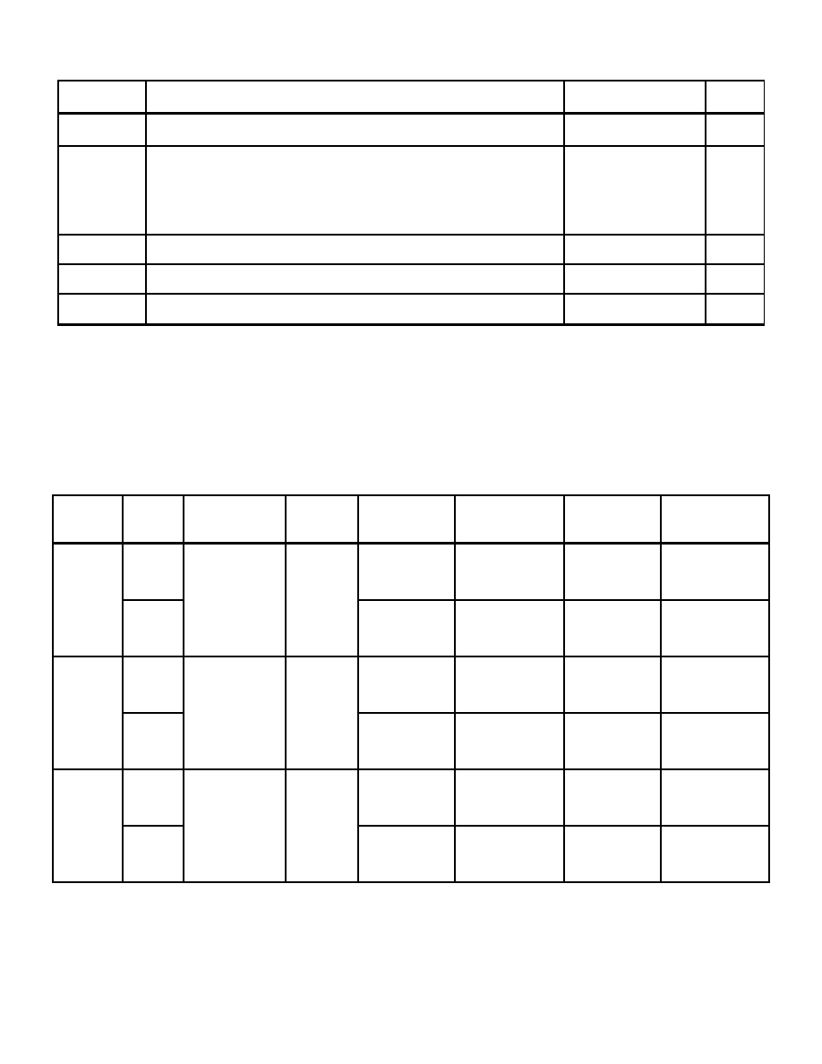
ABSOLUTE MAXIMUM RATINGS1
SYMBOL
RATING
RANGE
UNITS
VTERM
Terminal Voltage with respect to Vss
-0.52 to 3.9
V
Tc
Operating Temperature
I = Industrial
R = Extended
T = Military
M = Military, Screened
-40 to +85
-55 to +110
-55 to +125
°C
TSTG
Storage Temperature
-55 to +125
°C
IIN
DC Input Current
±20
mA
IOUT
DC Output Current 4
±20
mA
Notes:
1. Stresses above those listed under "AbsoluteMaximums Rating" may cause permanent damage to the device. This is a stress rating only
and functional operation of the device at these or any other conditions above those indicated in the operational sections of this
specification is not implied. Exposure to absolute maximum rating conditions for extended periods may affect device reliability.
2. VIN minimum = -2.0V for pulse width less than 15nS. VIN maximum should not exceed +3.95 Volts.
3. When VIN < 0V or VIN > VccIO.
4. No more than one output should be shorted at one time. Duration of the short should not exceed more than 30 second.
RECOMMENDED OPERATING CONDITIONS
GRADE
CPU
SPEED
TEMP
(CASE)
Vss
VccInt
VccIO
VccP
VccJ
Industrial
750
MHz
-40°C to+85°C
0 V
1.3 V ± 50 mV
3.3 V ± 150 mV
or
2.5 V ± 200 mV
1.3 V ± 50 mV
3.3 V ± 150 mV
or
2.5 V ± 200 mV
668
MHz
1.3 V ± 50 mV
3.3 V ± 150 mV
or
2.5 V ± 200 mV
1.3 V ± 50 mV
3.3 V ± 150 mV
or
2.5 V ± 200 mV
Extended
750
MHz
-55°C to +110°C
0 V
1.3 V ± 50 mV
3.3 V ± 150 mV
or
2.5 V ± 200 mV
1.3 V ± 50 mV
3.3 V ± 150 mV
or
2.5 V ± 200 mV
668
MHz
1.3 V ± 50 mV
3.3 V ± 150 mV
or
2.5 V ± 200 mV
1.3 V ± 50 mV
3.3 V ± 150 mV
or
2.5 V ± 200 mV
Military
750
MHz
-55°C to +125°C
Note 5
0 V
1.3 V ± 50 mV
3.3 V ± 150 mV
or
2.5 V ± 200 mV
1.3 V ± 50 mV
3.3 V ± 150 mV
or
2.5 V ± 200 mV
668
MHz
1.3 V ± 50 mV
3.3 V ± 150 mV
or
2.5 V ± 200 mV
1.3 V ± 50 mV
3.3 V ± 150 mV
or
2.5 V ± 200 mV
Notes
1. VccIO should not exceed VccInt by greater than 2.5 V during the power-up sequence.
2. Applying a logic high state to any I/O pin before VccInt becomes stable is not recommended.
3. As specified in IEEE 1149.1 (JTAG), the JTMS pin must be held high during reset to avoid entering JTAG test mode. Refer to the RM79xx
User Manual.
4. VccP must be connected to VccInt through a passive filter circuit. See RM79xx User Manual fo rrecommended circuit.
5. Contact factory for military temperature range products (CQFP hermetic MCM packages will be screened at -55°C to + 125°C).
相關(guān)PDF資料 |
PDF描述 |
|---|---|
| MIP7965-750F17T | 64-BIT, 750 MHz, MICROPROCESSOR, CQFP208 |
| MIP7965-668F24M | 64-BIT, 668 MHz, MICROPROCESSOR, CQFP208 |
| MIP7965-750F17I | 64-BIT, 750 MHz, MICROPROCESSOR, CQFP208 |
| MIP7965-668B1R | 64-BIT, 668 MHz, MICROPROCESSOR, PBGA256 |
| MJ80C51UXXX-36 | 8-BIT, MROM, 36 MHz, MICROCONTROLLER, CQCC44 |
相關(guān)代理商/技術(shù)參數(shù) |
參數(shù)描述 |
|---|---|
| MIP803 | 制造商:PANASONIC 制造商全稱:Panasonic Semiconductor 功能描述:Silicon MOS IC |
| MIP804 | 制造商:PANASONIC 制造商全稱:Panasonic Semiconductor 功能描述:Silicon MOS IC |
| MIP805 | 制造商:PANASONIC 制造商全稱:Panasonic Semiconductor 功能描述:Silicon MOS IC |
| MIPAQ | 制造商:INFINEON 制造商全稱:Infineon Technologies AG 功能描述:Infi neon’s functional IGBT module family |
| MI-PC201-IWY-CC | 制造商:Vicor Corporation 功能描述:MI-PC Series 100W Dual Output 5V 12V DC-DC |
發(fā)布緊急采購,3分鐘左右您將得到回復(fù)。