- 您現(xiàn)在的位置:買賣IC網(wǎng) > PDF目錄26808 > MC74LCX2952SD (ON SEMICONDUCTOR) LVC/LCX/Z SERIES, 8-BIT REGISTERED TRANSCEIVER, TRUE OUTPUT, PDSO24 PDF資料下載
參數(shù)資料
| 型號: | MC74LCX2952SD |
| 廠商: | ON SEMICONDUCTOR |
| 元件分類: | 總線收發(fā)器 |
| 英文描述: | LVC/LCX/Z SERIES, 8-BIT REGISTERED TRANSCEIVER, TRUE OUTPUT, PDSO24 |
| 封裝: | PLASTIC, SSOP-24 |
| 文件頁數(shù): | 29/43頁 |
| 文件大?。?/td> | 383K |
| 代理商: | MC74LCX2952SD |
第1頁第2頁第3頁第4頁第5頁第6頁第7頁第8頁第9頁第10頁第11頁第12頁第13頁第14頁第15頁第16頁第17頁第18頁第19頁第20頁第21頁第22頁第23頁第24頁第25頁第26頁第27頁第28頁當前第29頁第30頁第31頁第32頁第33頁第34頁第35頁第36頁第37頁第38頁第39頁第40頁第41頁第42頁第43頁
Reliability Information
LCX DATA
BR1339 — REV 3
245
MOTOROLA
Process Qualification Information
PROCESS QUALIFICATION SUMMARY
The H4C “plus” 75% CMOS (double layer metal)
process qualification consisted of intrinsic reliability
testing (Electromigration, Hot Carrier Injection, and
Dielectric Breakdown) and extrinsic reliability testing
(High Temperature Bias, Temperature Cycling, and
Pressure Temperature Humidity).
The intrinsic reliability measures indicate no significant
degradation over the lifetime of the device. Extrinsic
reliability for the process resulted in zero failures.
INTRINSIC RELIABILITY RESULTS
DEVICE QUALIFICATION
Electromigration
Electromigration evaluation of MOS 6 metals used in the
H4C ”plus” 75% CMOS (double layer metal) process
revealed an acceptable metallization process for a minimum
lifetime of 10 years at 100
°C with < .01% cumulative failures.
Hot Carrier Injection
HCI test (low temperature electrical stress) results indicate
less than 10% change in transconductance over the lifetime
of the transistor.
Dielectric Breakdown
The current conduction and QBD (charge breakdown)
data taken in MOS 6 was used to calculate an intrinsic gate
oxide lifetime of 1364 years. This estimated lifetime greatly
exceeds the expected lifetime of the device.
EXTRINSIC RELIABILITY RESULTS/DATA
PROCESS QUALIFICATION
The reliability testing consisted of High Temperature Bias
(145
°C, 3.6V bias), Temperature Cycling (–65°C to 150°C),
and PTH (121
°C, 15PSIG, & 100% RH). Samples from three
wafer lots were tested.
One wafer lot was a metal/dielectric split lot. The metal
and dielectric layers were run at the maximum and minimum
thickness specifications in order to account for step coverage
extremes.
The second wafer lot was a Vt/Leff split lot. The Vt and
Leff were run at minimum and maximum specifications in
order to account for extremes in leakage, speed, and
translation window.
The remaining lot was a nominal lot. Zero process related
rejects occurred after 504 hours of op–life, 600 temp cycles,
and 240 hours of PTH. (The device failure in time (FIT) was
calculated based on HTB results at 14.4; stress temp =
145
°C; activation energy = 0.7eV).
The H4C “plus” 75% CMOS (double layer metal) process
in MOS 6 was qualified and approved in light of the results of
the above intrinsic and extrinsic reliability results.
Package Qualification
MC74LCX family is being offered in SOIC, SSOP and TSSOP packaging. As the TSSOP package is a newer technology, a
qualification summary has been included in this report. All reliability tests have passed successfully, including preconditioning
tests used to simulate customer board mount processes (see below). Furthermore, based on reliability results, drypack* is not
required for this package type.
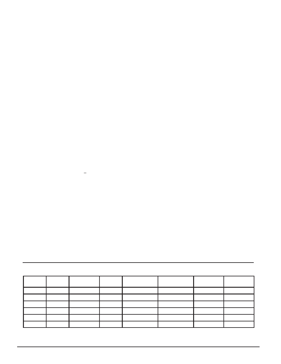
Package Qualification Summary
TSSOP
leads
Op Life
Temperature
Cycle
HAST
Surface Mount
Preconditioning
Solderability
Marking
Permanency
Physical
Dimension
14
PASS
PASS
PASS
PASS
PASS
PASS
PASS
16
PASS
PASS
PASS
PASS
PASS
PASS
PASS
20
PASS
PASS
PASS
PASS
PASS
PASS
PASS
24
PASS
PASS
PASS
PASS
PASS
PASS
PASS
48
PASS
PASS
PASS
PASS*
PASS
PASS
PASS
56
PASS
PASS
PASS
PASS*
PASS
PASS
PASS
* 48 and 56 lead TSSOP packages are moisture class level 2 and require drypack. Moisture class level 1 qualification is in progress – upon
successful completion, the 48–lead and 56–lead packages will no longer require dry pack.
相關(guān)PDF資料 |
PDF描述 |
|---|---|
| MC74LCX373DTR2 | LVC/LCX/Z SERIES, 8-BIT DRIVER, TRUE OUTPUT, PDSO20 |
| MC74LCX373MR2 | LVC/LCX/Z SERIES, 8-BIT DRIVER, TRUE OUTPUT, PDSO20 |
| MC74LCX540MR2 | LVC/LCX/Z SERIES, 8-BIT DRIVER, INVERTED OUTPUT, PDSO20 |
| MC74LCX540SDR2 | LVC/LCX/Z SERIES, 8-BIT DRIVER, INVERTED OUTPUT, PDSO20 |
| MC74LCX541DTR2 | LVC/LCX/Z SERIES, 8-BIT DRIVER, TRUE OUTPUT, PDSO20 |
相關(guān)代理商/技術(shù)參數(shù) |
參數(shù)描述 |
|---|---|
| MC74LCX32D | 制造商:Rochester Electronics LLC 功能描述:- Bulk |
| MC74LCX32DR2 | 功能描述:邏輯門 2-3.6V Quad 2-Input RoHS:否 制造商:Texas Instruments 產(chǎn)品:OR 邏輯系列:LVC 柵極數(shù)量:2 線路數(shù)量(輸入/輸出):2 / 1 高電平輸出電流:- 16 mA 低電平輸出電流:16 mA 傳播延遲時間:3.8 ns 電源電壓-最大:5.5 V 電源電壓-最小:1.65 V 最大工作溫度:+ 125 C 安裝風格:SMD/SMT 封裝 / 箱體:DCU-8 封裝:Reel |
| MC74LCX32DR2G | 功能描述:邏輯門 2-3.6V Quad 2-Input AND RoHS:否 制造商:Texas Instruments 產(chǎn)品:OR 邏輯系列:LVC 柵極數(shù)量:2 線路數(shù)量(輸入/輸出):2 / 1 高電平輸出電流:- 16 mA 低電平輸出電流:16 mA 傳播延遲時間:3.8 ns 電源電壓-最大:5.5 V 電源電壓-最小:1.65 V 最大工作溫度:+ 125 C 安裝風格:SMD/SMT 封裝 / 箱體:DCU-8 封裝:Reel |
| MC74LCX32DT | 功能描述:邏輯門 2-3.6V Quad 2-Input RoHS:否 制造商:Texas Instruments 產(chǎn)品:OR 邏輯系列:LVC 柵極數(shù)量:2 線路數(shù)量(輸入/輸出):2 / 1 高電平輸出電流:- 16 mA 低電平輸出電流:16 mA 傳播延遲時間:3.8 ns 電源電壓-最大:5.5 V 電源電壓-最小:1.65 V 最大工作溫度:+ 125 C 安裝風格:SMD/SMT 封裝 / 箱體:DCU-8 封裝:Reel |
| MC74LCX32DTEL | 制造商:Rochester Electronics LLC 功能描述:- Bulk |
發(fā)布緊急采購,3分鐘左右您將得到回復(fù)。