- 您現(xiàn)在的位置:買賣IC網(wǎng) > PDF目錄371054 > MC68HSC705C8A (Motorola, Inc.) HCMOS Microcontroller Unit PDF資料下載
參數(shù)資料
| 型號: | MC68HSC705C8A |
| 廠商: | Motorola, Inc. |
| 英文描述: | HCMOS Microcontroller Unit |
| 中文描述: | HCMOS微控制器 |
| 文件頁數(shù): | 202/222頁 |
| 文件大小: | 2253K |
| 代理商: | MC68HSC705C8A |
第1頁第2頁第3頁第4頁第5頁第6頁第7頁第8頁第9頁第10頁第11頁第12頁第13頁第14頁第15頁第16頁第17頁第18頁第19頁第20頁第21頁第22頁第23頁第24頁第25頁第26頁第27頁第28頁第29頁第30頁第31頁第32頁第33頁第34頁第35頁第36頁第37頁第38頁第39頁第40頁第41頁第42頁第43頁第44頁第45頁第46頁第47頁第48頁第49頁第50頁第51頁第52頁第53頁第54頁第55頁第56頁第57頁第58頁第59頁第60頁第61頁第62頁第63頁第64頁第65頁第66頁第67頁第68頁第69頁第70頁第71頁第72頁第73頁第74頁第75頁第76頁第77頁第78頁第79頁第80頁第81頁第82頁第83頁第84頁第85頁第86頁第87頁第88頁第89頁第90頁第91頁第92頁第93頁第94頁第95頁第96頁第97頁第98頁第99頁第100頁第101頁第102頁第103頁第104頁第105頁第106頁第107頁第108頁第109頁第110頁第111頁第112頁第113頁第114頁第115頁第116頁第117頁第118頁第119頁第120頁第121頁第122頁第123頁第124頁第125頁第126頁第127頁第128頁第129頁第130頁第131頁第132頁第133頁第134頁第135頁第136頁第137頁第138頁第139頁第140頁第141頁第142頁第143頁第144頁第145頁第146頁第147頁第148頁第149頁第150頁第151頁第152頁第153頁第154頁第155頁第156頁第157頁第158頁第159頁第160頁第161頁第162頁第163頁第164頁第165頁第166頁第167頁第168頁第169頁第170頁第171頁第172頁第173頁第174頁第175頁第176頁第177頁第178頁第179頁第180頁第181頁第182頁第183頁第184頁第185頁第186頁第187頁第188頁第189頁第190頁第191頁第192頁第193頁第194頁第195頁第196頁第197頁第198頁第199頁第200頁第201頁當(dāng)前第202頁第203頁第204頁第205頁第206頁第207頁第208頁第209頁第210頁第211頁第212頁第213頁第214頁第215頁第216頁第217頁第218頁第219頁第220頁第221頁第222頁
Technical Data
MC68HC705C8A
—
Rev. 3
202
MC68HSC705C8A
MOTOROLA
MC68HSC705C8A
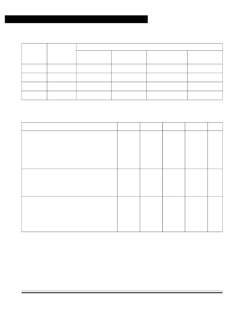
A.3 5.0-Volt High-Speed DC Electrical Characteristics
Table A-1. Programmable COP Timeout Period Selection
CM1:CM0
COP
Timeout
Rate
Programmable COP Timeout Period
f
OSC
= 8.0 MHz
f
OP
= 4.0 MHz
f
OSC
= 4.0 MHz
f
OP
= 2.0 MHz
f
OSC
= 3.5795 MHz
f
OP
= 1.7897 MHz
f
OSC
= 2.0 MHz
f
OP
= 1.0 MHz
00
f
OP
÷
2
15
8.192 ms
16.38 ms
18.31 ms
32.77 ms
01
f
OP
÷
2
17
32.77 ms
65.54 ms
73.24 ms
131.07 ms
10
f
OP
÷
2
19
131.07 ms
262.14 ms
292.95 ms
524.29 ms
11
f
OP
÷
÷
2
21
524.29 ms
1.048 s
1.172 s
2.097 s
Characteristic
(1)
1. V
DD
= 5 V
±
10%; V
SS
= 0 Vdc, T
A
= T
L
to T
H
, unless otherwise noted
2. Typical values reflect average measurements at midpoint of voltage range at 25
°
C.
3. I
DD
measured with port B pullup devices disabled.
4. Run (operating) I
DD
measured using external square wave clock source (f
OSC
= 8.0 MHz). All inputs 0.2 V from rail. No dc
loads. Less than 50 pF on all outputs. C
L
= 20 pF on OSC2. OSC2 capacitance linearly affects run I
DD
.
5. Wait I
DD
measured using external square wave clock source (f
OSC
= 8.0 MHz). All inputs 0.2 V from rail. No dc loads. Less
than 50 pF on all outputs. C
L
= 20 pF on OSC2. V
IL
= 0.2 V, V
IH
= V
DD
–
0.2 V. All ports configured as inputs. SPI and SCI
disabled. If SPI and SCI enabled, add 10% current draw. OSC2 capacitance linearly affects wait I
DD
.
6. Stop I
DD
measured with OSC1 = V
DD
. All ports configured as inputs. V
IL
= 0.2 V, V
IH
= V
DD
–
0.2 V.
Symbol
Min
Typ
(2)
Max
Unit
Output high voltage
I
Load
=
–
0.8 mA
PA7
–
PA0, PB7
–
PB0, PC6
–
PC0, TCMP
I
Load
=
–
1.6 mA
PD4
–
PD1
I
Load
=
–
5.0 mA
PC7
V
OH
V
DD
–
0.8
—
—
—
—
—
—
V
Output low voltage
I
Load
= 1.6 mA
PA7
–
PA0, PB7
–
PB0, PC6
–
PC0, PD4
–
PD1
I
Load
= 20 mA
PC7
V
OL
—
—
—
—
0.4
0.4
V
Supply current
(3)
Run
(4)
Wait
(5)
Stop
(6)
25
°
C
–
40
°
C to +85
°
C
I
DD
—
—
—
—
5.92
2.27
5
2.0
14
7.0
50
50
mA
mA
μ
A
μ
A
相關(guān)PDF資料 |
PDF描述 |
|---|---|
| MC68HSC705C8ACB | M68HC05 MICROCONTROLLERS |
| MC68HSC705C8ACFB | M68HC05 MICROCONTROLLERS |
| MC68HSC705C8ACFN | M68HC05 MICROCONTROLLERS |
| MC68HSC705C8ACP | M68HC05 MICROCONTROLLERS |
| MC68LC302 | 32-Bit Microprocessor(32位微處理器) |
相關(guān)代理商/技術(shù)參數(shù) |
參數(shù)描述 |
|---|---|
| MC68HSC705C8ACFB | 制造商:Rochester Electronics LLC 功能描述:8 BIT MCU, 304 BYTES RAM - Bulk |
| MC68HSC705C8ACP | 制造商:Rochester Electronics LLC 功能描述: 制造商:Freescale Semiconductor 功能描述: |
| MC68HSC705C8ACS | 制造商:Rochester Electronics LLC 功能描述:- Bulk |
| MC68HSC705J1ACDW | 制造商:Rochester Electronics LLC 功能描述:- Bulk |
| MC68HSC705J1ACP | 制造商:Rochester Electronics LLC 功能描述:8 BIT MCU, 64 BYTES RAM - Bulk |
發(fā)布緊急采購,3分鐘左右您將得到回復(fù)。