- 您現(xiàn)在的位置:買賣IC網(wǎng) > PDF目錄45233 > MC68HC12BE32MFU8 (MOTOROLA INC) 16-BIT, MROM, 8 MHz, MICROCONTROLLER, PQFP80 PDF資料下載
參數(shù)資料
| 型號(hào): | MC68HC12BE32MFU8 |
| 廠商: | MOTOROLA INC |
| 元件分類: | 微控制器/微處理器 |
| 英文描述: | 16-BIT, MROM, 8 MHz, MICROCONTROLLER, PQFP80 |
| 封裝: | QFP-80 |
| 文件頁(yè)數(shù): | 246/362頁(yè) |
| 文件大小: | 4604K |
| 代理商: | MC68HC12BE32MFU8 |
第1頁(yè)第2頁(yè)第3頁(yè)第4頁(yè)第5頁(yè)第6頁(yè)第7頁(yè)第8頁(yè)第9頁(yè)第10頁(yè)第11頁(yè)第12頁(yè)第13頁(yè)第14頁(yè)第15頁(yè)第16頁(yè)第17頁(yè)第18頁(yè)第19頁(yè)第20頁(yè)第21頁(yè)第22頁(yè)第23頁(yè)第24頁(yè)第25頁(yè)第26頁(yè)第27頁(yè)第28頁(yè)第29頁(yè)第30頁(yè)第31頁(yè)第32頁(yè)第33頁(yè)第34頁(yè)第35頁(yè)第36頁(yè)第37頁(yè)第38頁(yè)第39頁(yè)第40頁(yè)第41頁(yè)第42頁(yè)第43頁(yè)第44頁(yè)第45頁(yè)第46頁(yè)第47頁(yè)第48頁(yè)第49頁(yè)第50頁(yè)第51頁(yè)第52頁(yè)第53頁(yè)第54頁(yè)第55頁(yè)第56頁(yè)第57頁(yè)第58頁(yè)第59頁(yè)第60頁(yè)第61頁(yè)第62頁(yè)第63頁(yè)第64頁(yè)第65頁(yè)第66頁(yè)第67頁(yè)第68頁(yè)第69頁(yè)第70頁(yè)第71頁(yè)第72頁(yè)第73頁(yè)第74頁(yè)第75頁(yè)第76頁(yè)第77頁(yè)第78頁(yè)第79頁(yè)第80頁(yè)第81頁(yè)第82頁(yè)第83頁(yè)第84頁(yè)第85頁(yè)第86頁(yè)第87頁(yè)第88頁(yè)第89頁(yè)第90頁(yè)第91頁(yè)第92頁(yè)第93頁(yè)第94頁(yè)第95頁(yè)第96頁(yè)第97頁(yè)第98頁(yè)第99頁(yè)第100頁(yè)第101頁(yè)第102頁(yè)第103頁(yè)第104頁(yè)第105頁(yè)第106頁(yè)第107頁(yè)第108頁(yè)第109頁(yè)第110頁(yè)第111頁(yè)第112頁(yè)第113頁(yè)第114頁(yè)第115頁(yè)第116頁(yè)第117頁(yè)第118頁(yè)第119頁(yè)第120頁(yè)第121頁(yè)第122頁(yè)第123頁(yè)第124頁(yè)第125頁(yè)第126頁(yè)第127頁(yè)第128頁(yè)第129頁(yè)第130頁(yè)第131頁(yè)第132頁(yè)第133頁(yè)第134頁(yè)第135頁(yè)第136頁(yè)第137頁(yè)第138頁(yè)第139頁(yè)第140頁(yè)第141頁(yè)第142頁(yè)第143頁(yè)第144頁(yè)第145頁(yè)第146頁(yè)第147頁(yè)第148頁(yè)第149頁(yè)第150頁(yè)第151頁(yè)第152頁(yè)第153頁(yè)第154頁(yè)第155頁(yè)第156頁(yè)第157頁(yè)第158頁(yè)第159頁(yè)第160頁(yè)第161頁(yè)第162頁(yè)第163頁(yè)第164頁(yè)第165頁(yè)第166頁(yè)第167頁(yè)第168頁(yè)第169頁(yè)第170頁(yè)第171頁(yè)第172頁(yè)第173頁(yè)第174頁(yè)第175頁(yè)第176頁(yè)第177頁(yè)第178頁(yè)第179頁(yè)第180頁(yè)第181頁(yè)第182頁(yè)第183頁(yè)第184頁(yè)第185頁(yè)第186頁(yè)第187頁(yè)第188頁(yè)第189頁(yè)第190頁(yè)第191頁(yè)第192頁(yè)第193頁(yè)第194頁(yè)第195頁(yè)第196頁(yè)第197頁(yè)第198頁(yè)第199頁(yè)第200頁(yè)第201頁(yè)第202頁(yè)第203頁(yè)第204頁(yè)第205頁(yè)第206頁(yè)第207頁(yè)第208頁(yè)第209頁(yè)第210頁(yè)第211頁(yè)第212頁(yè)第213頁(yè)第214頁(yè)第215頁(yè)第216頁(yè)第217頁(yè)第218頁(yè)第219頁(yè)第220頁(yè)第221頁(yè)第222頁(yè)第223頁(yè)第224頁(yè)第225頁(yè)第226頁(yè)第227頁(yè)第228頁(yè)第229頁(yè)第230頁(yè)第231頁(yè)第232頁(yè)第233頁(yè)第234頁(yè)第235頁(yè)第236頁(yè)第237頁(yè)第238頁(yè)第239頁(yè)第240頁(yè)第241頁(yè)第242頁(yè)第243頁(yè)第244頁(yè)第245頁(yè)當(dāng)前第246頁(yè)第247頁(yè)第248頁(yè)第249頁(yè)第250頁(yè)第251頁(yè)第252頁(yè)第253頁(yè)第254頁(yè)第255頁(yè)第256頁(yè)第257頁(yè)第258頁(yè)第259頁(yè)第260頁(yè)第261頁(yè)第262頁(yè)第263頁(yè)第264頁(yè)第265頁(yè)第266頁(yè)第267頁(yè)第268頁(yè)第269頁(yè)第270頁(yè)第271頁(yè)第272頁(yè)第273頁(yè)第274頁(yè)第275頁(yè)第276頁(yè)第277頁(yè)第278頁(yè)第279頁(yè)第280頁(yè)第281頁(yè)第282頁(yè)第283頁(yè)第284頁(yè)第285頁(yè)第286頁(yè)第287頁(yè)第288頁(yè)第289頁(yè)第290頁(yè)第291頁(yè)第292頁(yè)第293頁(yè)第294頁(yè)第295頁(yè)第296頁(yè)第297頁(yè)第298頁(yè)第299頁(yè)第300頁(yè)第301頁(yè)第302頁(yè)第303頁(yè)第304頁(yè)第305頁(yè)第306頁(yè)第307頁(yè)第308頁(yè)第309頁(yè)第310頁(yè)第311頁(yè)第312頁(yè)第313頁(yè)第314頁(yè)第315頁(yè)第316頁(yè)第317頁(yè)第318頁(yè)第319頁(yè)第320頁(yè)第321頁(yè)第322頁(yè)第323頁(yè)第324頁(yè)第325頁(yè)第326頁(yè)第327頁(yè)第328頁(yè)第329頁(yè)第330頁(yè)第331頁(yè)第332頁(yè)第333頁(yè)第334頁(yè)第335頁(yè)第336頁(yè)第337頁(yè)第338頁(yè)第339頁(yè)第340頁(yè)第341頁(yè)第342頁(yè)第343頁(yè)第344頁(yè)第345頁(yè)第346頁(yè)第347頁(yè)第348頁(yè)第349頁(yè)第350頁(yè)第351頁(yè)第352頁(yè)第353頁(yè)第354頁(yè)第355頁(yè)第356頁(yè)第357頁(yè)第358頁(yè)第359頁(yè)第360頁(yè)第361頁(yè)第362頁(yè)
General Description
Data Sheet
M68HC12B Family — Rev. 9.0
32
General Description
MOTOROLA
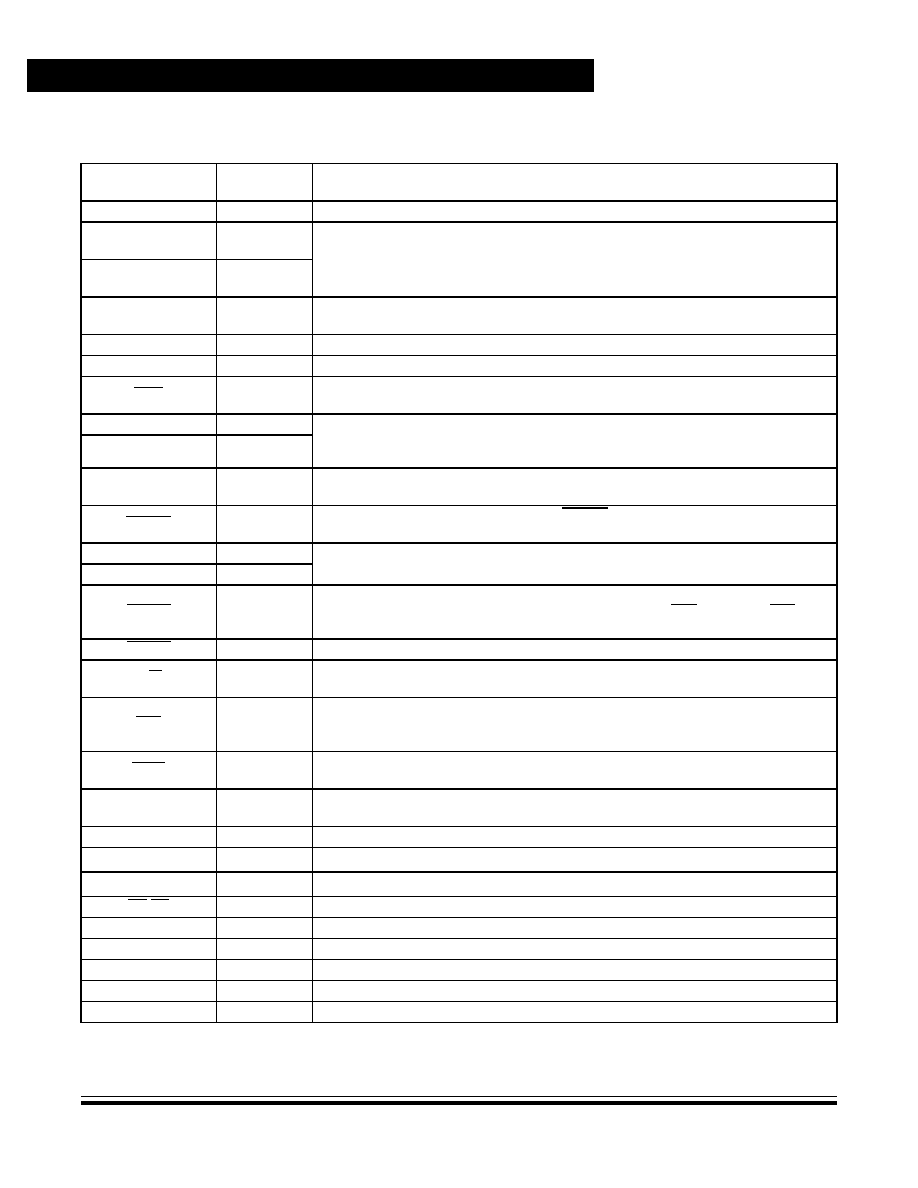
Table 1-3. Signal Description Summary
Pin
Name
Pin
Number
Description
PW3–PW0
3–6
Pulse-width modulator channel outputs
ADDR7–ADDR0
DATA7–DATA0
25–18
External bus pins share function with general-purpose I/O ports A and B. In single-chip
modes, the pins can be used for I/O. In expanded modes, the pins are used for the
external buses.
ADDR15–ADDR8
DATA15–DATA8
46–39
IOC7–IOC0
16–12, 9–7
Pins used for input capture and output compare in the timer and pulse accumulator
subsystem
PAI
16
Pulse accumulator input
AN7–AN0
58–51
Analog inputs for the analog-to-digital conversion module
DBE
26
Data bus control and, in expanded mode, enables the drive control of external buses
during external reads
MODB, MODA
27, 28
State of mode select pins during reset determines the initial operating mode of the
MCU. After reset, MODB and MODA can be configured as instruction queue tracking
signals IPIPE1 and IPIPE0 or as general-purpose I/O pins.
IPIPE1, IPIPE0
27, 28
ECLK
29
E-clock is the output connection for the external bus clock. ECLK is used as a timing
reference and for address demultiplexing.
RESET
32
An active low bidirectional control signal, RESET acts as an input to initialize the MCU
to a known startup state and an output when COP or clock monitor causes a reset.
EXTAL
33
Crystal driver and external clock input pins. On reset all the device clocks are derived
from the EXTAL input frequency. XTAL is the crystal output.
XTAL
34
LSTRB
35
Low byte strobe (0 = low byte valid), in all modes this pin can be used as I/O. The low
strobe function is the exclusive-NOR of A0 and the internal SZ8 signal. The SZ8
internal signal indicates the size 16/8 access.
TAGLO
35
Pin used in instruction tagging
R/W
36
Indicates direction of data on expansion bus; shares function with general-purpose I/O;
read/write in expanded modes
IRQ
37
Maskable interrupt request input provides a means of applying asynchronous interrupt
requests to the MCU. Either falling edge-sensitive triggering or level-sensitive
triggering is program selectable (INTCR register).
XIRQ
38
Provides a means of requesting asynchronous non-maskable interrupt requests after
reset initialization
BKGD
17
Single-wire background interface pin is dedicated to the background debug function.
During reset, this pin determines special or normal operating mode.
TAGHI
17
Pin used in instruction tagging
DLCRx/RxCAN(1)
76
BDLC receive pin
DLCTx/TxCAN(1)
75
BDLC transmit pin
CS/SS
68
Slave-select output for SPI master mode; input for slave mode or master mode
SCK
67
Serial clock for SPI system
SDO/MOSI
66
Master out/slave in pin for serial peripheral interface
SDI/MISO
65
Master in/slave out pin for serial peripheral interface
TxD0
62
SCI transmit pin
RxD0
61
SCI receive pin
1. The RxCAN and TxCAN designations are for the MC68HC(9)12BC32 only.
相關(guān)PDF資料 |
PDF描述 |
|---|---|
| MC68HC12BE32VFU | 16-BIT, MROM, 8 MHz, MICROCONTROLLER, PQFP80 |
| MC68HC912B32CFU | 16-BIT, FLASH, 8 MHz, MICROCONTROLLER, PQFP80 |
| MC68HC16S2CPU25 | 16-BIT, 25.17 MHz, MICROCONTROLLER, PQFP100 |
| MC68HC16S2CPU20 | 16-BIT, 20.97 MHz, MICROCONTROLLER, PQFP100 |
| MC68HC16Z1CFV25 | 16-BIT, 25 MHz, MICROCONTROLLER, PQFP144 |
相關(guān)代理商/技術(shù)參數(shù) |
參數(shù)描述 |
|---|---|
| MC68HC16Z1CAG | 制造商:Freescale Semiconductor 功能描述: |
| MC68HC16Z1CAG16 | 功能描述:16位微控制器 - MCU 16 BIT MCU 1K RAM RoHS:否 制造商:Texas Instruments 核心:RISC 處理器系列:MSP430FR572x 數(shù)據(jù)總線寬度:16 bit 最大時(shí)鐘頻率:24 MHz 程序存儲(chǔ)器大小:8 KB 數(shù)據(jù) RAM 大小:1 KB 片上 ADC:Yes 工作電源電壓:2 V to 3.6 V 工作溫度范圍:- 40 C to + 85 C 封裝 / 箱體:VQFN-40 安裝風(fēng)格:SMD/SMT |
| MC68HC16Z1CAG16 | 制造商:Freescale Semiconductor 功能描述:IC16-BIT MICROCONTROLLER |
| MC68HC16Z1CAG20 | 功能描述:16位微控制器 - MCU 16 BIT MCU 1K RAM RoHS:否 制造商:Texas Instruments 核心:RISC 處理器系列:MSP430FR572x 數(shù)據(jù)總線寬度:16 bit 最大時(shí)鐘頻率:24 MHz 程序存儲(chǔ)器大小:8 KB 數(shù)據(jù) RAM 大小:1 KB 片上 ADC:Yes 工作電源電壓:2 V to 3.6 V 工作溫度范圍:- 40 C to + 85 C 封裝 / 箱體:VQFN-40 安裝風(fēng)格:SMD/SMT |
| MC68HC16Z1CAG20 | 制造商:Freescale Semiconductor 功能描述:Microcontroller |
發(fā)布緊急采購(gòu),3分鐘左右您將得到回復(fù)。