- 您現(xiàn)在的位置:買賣IC網(wǎng) > PDF目錄45211 > MC68307CFG16 (MOTOROLA INC) 16-BIT, 16.67 MHz, MICROCONTROLLER, PQFP100 PDF資料下載
參數(shù)資料
| 型號: | MC68307CFG16 |
| 廠商: | MOTOROLA INC |
| 元件分類: | 微控制器/微處理器 |
| 英文描述: | 16-BIT, 16.67 MHz, MICROCONTROLLER, PQFP100 |
| 封裝: | PLASTIC, QFP-100 |
| 文件頁數(shù): | 30/264頁 |
| 文件大小: | 949K |
| 代理商: | MC68307CFG16 |
第1頁第2頁第3頁第4頁第5頁第6頁第7頁第8頁第9頁第10頁第11頁第12頁第13頁第14頁第15頁第16頁第17頁第18頁第19頁第20頁第21頁第22頁第23頁第24頁第25頁第26頁第27頁第28頁第29頁當前第30頁第31頁第32頁第33頁第34頁第35頁第36頁第37頁第38頁第39頁第40頁第41頁第42頁第43頁第44頁第45頁第46頁第47頁第48頁第49頁第50頁第51頁第52頁第53頁第54頁第55頁第56頁第57頁第58頁第59頁第60頁第61頁第62頁第63頁第64頁第65頁第66頁第67頁第68頁第69頁第70頁第71頁第72頁第73頁第74頁第75頁第76頁第77頁第78頁第79頁第80頁第81頁第82頁第83頁第84頁第85頁第86頁第87頁第88頁第89頁第90頁第91頁第92頁第93頁第94頁第95頁第96頁第97頁第98頁第99頁第100頁第101頁第102頁第103頁第104頁第105頁第106頁第107頁第108頁第109頁第110頁第111頁第112頁第113頁第114頁第115頁第116頁第117頁第118頁第119頁第120頁第121頁第122頁第123頁第124頁第125頁第126頁第127頁第128頁第129頁第130頁第131頁第132頁第133頁第134頁第135頁第136頁第137頁第138頁第139頁第140頁第141頁第142頁第143頁第144頁第145頁第146頁第147頁第148頁第149頁第150頁第151頁第152頁第153頁第154頁第155頁第156頁第157頁第158頁第159頁第160頁第161頁第162頁第163頁第164頁第165頁第166頁第167頁第168頁第169頁第170頁第171頁第172頁第173頁第174頁第175頁第176頁第177頁第178頁第179頁第180頁第181頁第182頁第183頁第184頁第185頁第186頁第187頁第188頁第189頁第190頁第191頁第192頁第193頁第194頁第195頁第196頁第197頁第198頁第199頁第200頁第201頁第202頁第203頁第204頁第205頁第206頁第207頁第208頁第209頁第210頁第211頁第212頁第213頁第214頁第215頁第216頁第217頁第218頁第219頁第220頁第221頁第222頁第223頁第224頁第225頁第226頁第227頁第228頁第229頁第230頁第231頁第232頁第233頁第234頁第235頁第236頁第237頁第238頁第239頁第240頁第241頁第242頁第243頁第244頁第245頁第246頁第247頁第248頁第249頁第250頁第251頁第252頁第253頁第254頁第255頁第256頁第257頁第258頁第259頁第260頁第261頁第262頁第263頁第264頁
System Integration Module
5-30
MC68307 USER’S MANUAL
MOTOROLA
CD2–CD0—Low-Power Clock Divider Ratio
Program these bits to specify the frequency of clock signal for the EC000 core processor
when CPU clock division is enabled by the CDEN bit.
After a cold reset , these bits are cleared, so the EC000 core would run at half the system
clock frequency, if the CDEN bit was set. These bits are unaffected by wake-up. For main
low-power sleep (LPEN) operation, the CD2–CD0 and CDEN bit values are ignored.
NOTE
The clock divider ratio should only be changed from one divider
value to another when the CDEN bit is zero, i.e. when the CPU
is operating at full speed. Changing from one reduced speed to
another is not recommended.
5.2.2 Chip Select Registers
Each of the four chip select units has two registers that define its specific operation. These
registers are a 16-bit base register (BR) and a 16-bit option register (OR) (e.g., BR0 and
OR0). These registers may be modified by the EC000 core. The BR should normally be
programmed after the OR since the BR contains the chip select enable bit. Programming
both registers at once using a long word write is also recommended.
5.2.2.1 BASE REGISTERS (BR3–BR0). These 16-bit registers consist of a base address
field, a read-write bit, a function code field and an enable bit.
FC2–FC0—Function Code Field
These bits are used to set the address space function code. The address compare logic
uses these bits to determine whether an address match exists within its address space
and, therefore, whether to assert the chip select line. Although the FC2–FC0 signals are
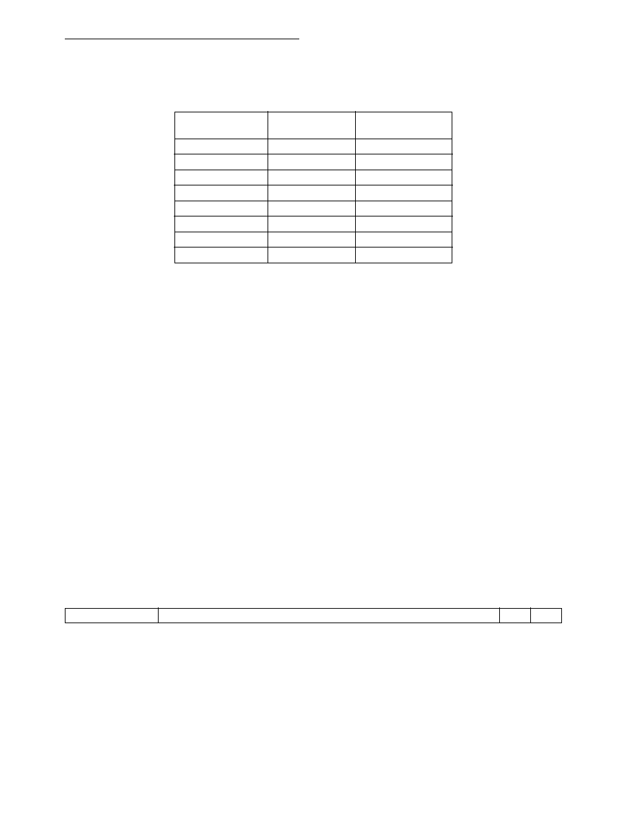
Value
Division Ratio
Frequency from
16MHz EXTAL
000
÷2
~8MHz
001
÷4
~4MHz
010
÷8
~2MHz
011
÷16
~1MHz
100
÷32
~512kHz
101
÷64
~256kHz
110
÷128
~128kHz
111
÷256
~64kHz
BR0, BR1, BR2, BR3
MBASE+$040, $044, $048, $04C
15
13
12
2
1
0
FC2
FC1
FC0
A23
A22
A21
A20
A19
A18
A17
A16
A15
A14
A13
RW
EN
RESET:
1
0
1
Read/Write
Supervisor or User
相關(guān)PDF資料 |
PDF描述 |
|---|---|
| MC68307PU16 | 16-BIT, 16.67 MHz, MICROCONTROLLER, PQFP100 |
| MC68307PU16V | 16-BIT, 16.67 MHz, MICROCONTROLLER, PQFP100 |
| MC68307FG16 | 16-BIT, 16.67 MHz, MICROCONTROLLER, PQFP100 |
| MC68322FT16 | 16-BIT, 16.667 MHz, RISC PROCESSOR, PQFP160 |
| MC68331CFC20B1 | 32-BIT, 20 MHz, MICROCONTROLLER, PQFP132 |
相關(guān)代理商/技術(shù)參數(shù) |
參數(shù)描述 |
|---|---|
| MC68307UM | 制造商:MOTOROLA 制造商全稱:Motorola, Inc 功能描述:Technical Summary Integrated Multiple-Bus Processor |
| MC68307V | 制造商:MOTOROLA 制造商全稱:Motorola, Inc 功能描述:Technical Summary Integrated Multiple-Bus Processor |
| MC68322 | 制造商:MOTOROLA 制造商全稱:Motorola, Inc 功能描述:Integrated Printer Processor |
| MC68322AD | 制造商:MOTOROLA 制造商全稱:Motorola, Inc 功能描述:Integrated Printer Processor |
| MC68322FT20 | 制造商:Rochester Electronics LLC 功能描述:- Bulk |
發(fā)布緊急采購,3分鐘左右您將得到回復(fù)。