- 您現(xiàn)在的位置:買賣IC網(wǎng) > PDF目錄378659 > MC145191DT (MOTOROLA INC) 1.1 GHz PLL Frequency Synthesizers PDF資料下載
參數(shù)資料
| 型號: | MC145191DT |
| 廠商: | MOTOROLA INC |
| 元件分類: | XO, clock |
| 英文描述: | 1.1 GHz PLL Frequency Synthesizers |
| 中文描述: | PLL FREQUENCY SYNTHESIZER, 1100 MHz, PDSO20 |
| 封裝: | TSSOP-20 |
| 文件頁數(shù): | 2/24頁 |
| 文件大小: | 341K |
| 代理商: | MC145191DT |
MC145190
MC145191
2
MOTOROLA
ENB
REFin
Din
CLK
REFout
fin
fin
OSC OR
4–STAGE
DIVIDER
(CONFIGURABLE)
20
1
18
19
11
10
OUTPUT A
INPUT
AMP
SELECT
LOGIC
3
13
24
13–STAGE R COUNTER
64/65
PRESCALER
MODULUS
CONTROL
LOGIC
12–STAGE
N COUNTER
6–STAGE
A COUNTER
INTERNAL
CONTROL
SHIFT
REGISTER
AND
CONTROL
LOGIC
STANDBY
LOGIC
POR
BitGrabber
A REGISTER
24 BITS
BitGrabber
C REGISTER
8 BITS
DOUBLE–BUFFERED
BitGrabber
R REGISTER
16 BITS
PHASE/FREQUENCY
DETECTOR B AND CONTROL
PHASE/FREQUENCY
DETECTOR A AND CONTROL
LOCK DETECTOR
AND CONTROL
6
12
4
2
LD
Rx
PDout
φ
R
φ
V
OUTPUT B
(OPEN–DRAIN
OUTPUT)
TEST 2
TEST 1
9
15
13
4
3
6
8
2
16
SUPPLY CONNECTIONS:
PIN 12 = VCC (V+ TO INPUT AMP AND 64/65 PRESCALER)
PIN 5 = VPD (V+ TO PHASE/FREQUENCY DETECTORS A AND B)
PIN 14 = VDD (V+ TO BALANCE OF CIRCUIT)
PIN 7 = GND (COMMON GROUND)
17
DATA OUT
fR
fV
PORT
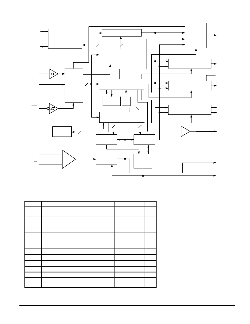
BLOCK DIAGRAM
MAXIMUM RATINGS*
(Voltages Referenced to GND, unless otherwise stated)
Symbol
Parameter
Value
Unit
VCC,
VDD
VPD
DC Supply Voltage (Pins 12 and 14)
– 0.5 to + 6.0
V
DC Supply Voltage (Pin 5)
MC145190
MC145191
VDD – 0.5 to + 9.5
VDD – 0.5 to + 6.0
– 0.5 to VDD + 0.5
– 0.5 to VDD + 0.5
V
Vin
Vout
DC Input Voltage
V
DC Output Voltage (except OUTPUT B, PDout,
φ
R,
φ
V)
DC Output Voltage (OUTPUT B, PDout,
φ
R,
φ
V)
DC Input Current, per Pin (Includes VPD)
DC Output Current, per Pin
V
Vout
Iin, IPD
Iout
IDD
PD
Tstg
TL
– 0.5 to VPD + 0.5
±
10
±
20
±
30
V
mA
mA
DC Supply Current, VDD and GND Pins
Power Dissipation, per Package
mA
300
mW
Storage Temperature
– 65 to + 150
°
C
°
C
Lead Temperature, 1 mm from Case for
10 seconds
260
* Maximum Ratings are those values beyond which damage to the device may occur.
Functional operation should be restricted to the limits in the Electrical Characteristics tables
or Pin Descriptions section.
This device contains protection circuitry to
guard against damage due to high static volt-
ages or electric fields. However, precautions
must be taken to avoid applications of any volt-
age higher than maximum rated voltages to
this high–impedance circuit.
相關(guān)PDF資料 |
PDF描述 |
|---|---|
| MC145191F | 1.1 GHz PLL Frequency Synthesizers |
| MC145192DT | 8-Pin High Frequency 4-Amp Sink Synchronous MOSFET Driver 8-SOIC -40 to 125 |
| MC145192 | Low-Voltage 1.1 GHz PLL Frequency Synthesizer |
| MC145192EVK | 8-Pin High Frequency 4-Amp Sink Synchronous MOSFET Driver 8-SON -40 to 125 |
| MC145192F | Low-Voltage 1.1 GHz PLL Frequency Synthesizer |
相關(guān)代理商/技術(shù)參數(shù) |
參數(shù)描述 |
|---|---|
| MC14519BCL | 制造商:Motorola Inc 功能描述: 制造商:Motorola Inc 功能描述:LOGIC MUX, QUAD, 2-INPUT, CMOS, 16 Pin, Ceramic, DIP |
| MC14519BD | 制造商:Rochester Electronics LLC 功能描述:- Bulk |
| MC14519BF | 制造商:Panasonic Industrial Company 功能描述:IC |
| MC1451CCP | 制造商:PMD 功能描述: |
| MC14520B | 制造商:Motorola Inc 功能描述: 制造商:ON Semiconductor 功能描述: |
發(fā)布緊急采購,3分鐘左右您將得到回復(fù)。