- 您現(xiàn)在的位置:買賣IC網(wǎng) > PDF目錄378659 > MC145191DT (MOTOROLA INC) 1.1 GHz PLL Frequency Synthesizers PDF資料下載
參數(shù)資料
| 型號: | MC145191DT |
| 廠商: | MOTOROLA INC |
| 元件分類: | XO, clock |
| 英文描述: | 1.1 GHz PLL Frequency Synthesizers |
| 中文描述: | PLL FREQUENCY SYNTHESIZER, 1100 MHz, PDSO20 |
| 封裝: | TSSOP-20 |
| 文件頁數(shù): | 19/24頁 |
| 文件大小: | 341K |
| 代理商: | MC145191DT |
MC145190
MC145191
MOTOROLA
19
F(s) =
ASSUMING GAIN A IS VERY LARGE, THEN:
Z(s) =
ζ
=
ω
n =
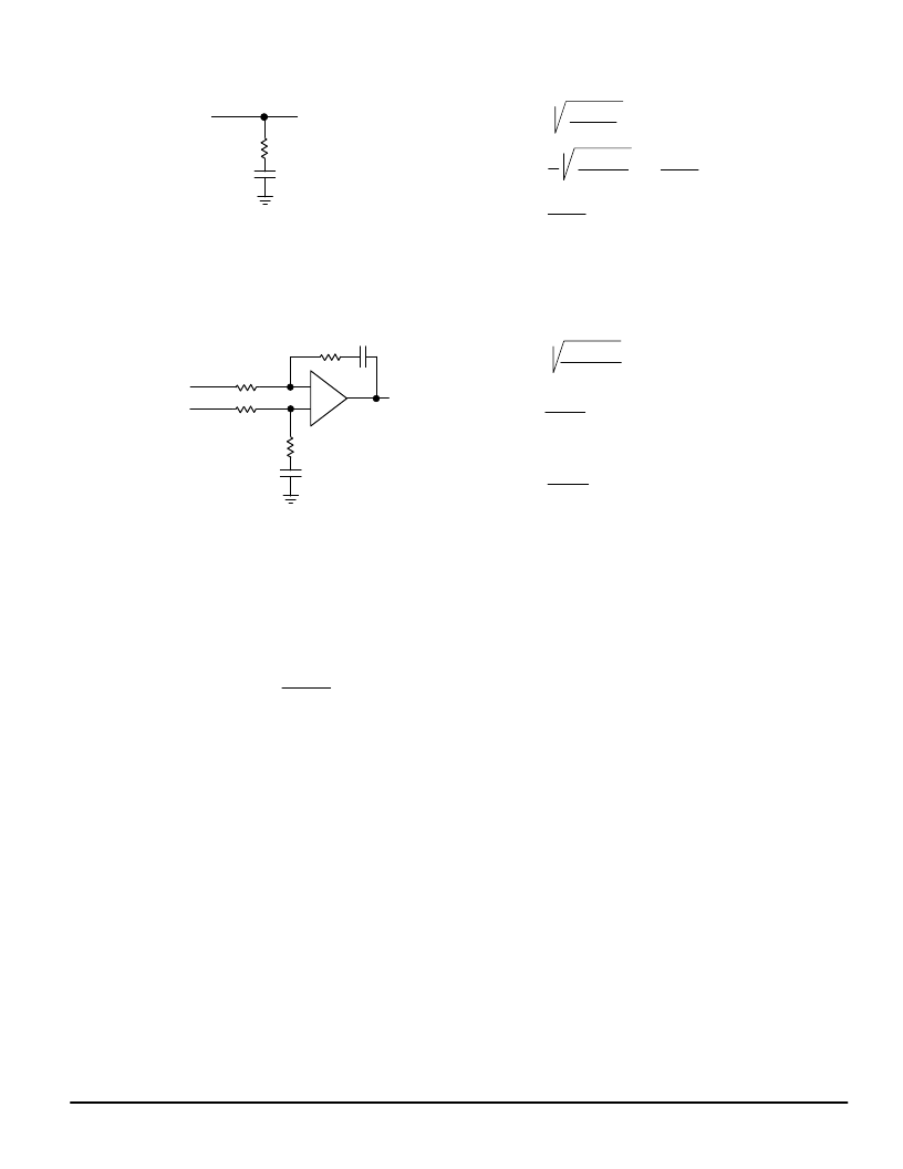
PHASE–LOCKED LOOP—LOW PASS FILTER DESIGN
(B)
A
C
R2
C
VCO
(A)
φ
R
φ
V
R1
R1
R2
K
φ
KVCO
NC
R
2
sC
ω
n =
K
φ
KVCO
NCR1
ζ
=
ω
nR2C
2
R2sC + 1
R1sC
NOTE:
For (B), R1 is frequently split into two series resistors; each resistor is equal to R1 divided by 2. A capacitor CC is then placed from
the midpoint to ground to further filter the error pulses. The value of CC should be such that the corner frequency of this network does
not significantly affect
ω
n.
* The
φ
R and
φ
V outputs are fed to an external combiner/loop filter. The
φ
R and
φ
V outputs swing rail–to–rail. Therefore, the user should be careful
not to exceed the common mode input range of the op amp used in the combiner/loop filter.
DEFINITIONS:
N = Total Division Ratio in Feedback Loop
K
φ
(Phase Detector Gain) = IPDout/2
π
amps per radian for PDout
K
φ
(Phase Detector Gain) = VPD/2
π
volts per radian for
φ
V and
φ
R
KVCO (VCO Transfer Function) =
2
π
fVCO
VVCO
For a nominal design starting point, the user might consider a damping factor
ζ
≈
0.7 and a natural loop frequency
ω
n
≈
(2
π
fR/50) where fR is
the frequency at the phase detector input. Larger
ω
n values result in faster loop lock times and, for similar sideband filtering, higher fR–related
VCO sidebands.
RECOMMENDED READING:
Gardner, Floyd M., Phaselock Techniques (second edition).New York, Wiley–Interscience, 1979.
Manassewitsch, Vadim, Frequency Synthesizers: Theory and Design (second edition). New York, Wiley–Interscience, 1980.
Blanchard, Alain, Phase–Locked Loops: Application to Coherent Receiver Design.New York, Wiley–Interscience, 1976.
Egan, William F., Frequency Synthesis by Phase Lock. New York, Wiley–Interscience, 1981.
Rohde, Ulrich L., Digital PLL Frequency Synthesizers Theory and Design. Englewood Cliffs, NJ, Prentice–Hall, 1983.
Berlin, Howard M., Design of Phase–Locked Loop Circuits, with Experiments.Indianapolis, Howard W. Sams and Co., 1978.
Kinley, Harold, The PLL Synthesizer Cookbook.Blue Ridge Summit, PA, Tab Books, 1980.
Seidman, Arthur H., Integrated Circuits Applications Handbook Chapter 17, pp. 538–586. New York, John Wiley & Sons.
Fadrhons, Jan, “Design and Analyze PLLs on a Programmable Calculator,” EDN March 5, 1980.
AN535, Phase–Locked Loop Design Fundamentals, Motorola Semiconductor Products, Inc., 1970.
AR254, Phase–Locked Loop Design Articles, Motorola Semiconductor Products, Inc., Reprinted with permission from
Electronic Design,1987.
AN1253/D, An Improved PLL Design Method Without
ω
n and
ζ
, Motorola Semiconductor Products, Inc., 1995.
–
+
KVCOC
N
K
φ
1 + sRC
NOTE:
For (A), using K
φ
in amps per radian with the filter’s impedance transfer function, Z(s), maintains units of volts per radian for the
detector/ filter combination. Additional sideband filtering can be accomplished by adding a capacitor C
′
across R. The corner
ω
c = 1/RC
′
should be chosen such that
ω
n is not significantly affected.
C
VCO
R
PDout
radians per volt
Either loop filter (A) or (B) is frequently followed by additional sideband filtering to further attenuate fR–related VCO sidebands. This additional
filtering may be active or passive.
=
ω
nRC
2
相關(guān)PDF資料 |
PDF描述 |
|---|---|
| MC145191F | 1.1 GHz PLL Frequency Synthesizers |
| MC145192DT | 8-Pin High Frequency 4-Amp Sink Synchronous MOSFET Driver 8-SOIC -40 to 125 |
| MC145192 | Low-Voltage 1.1 GHz PLL Frequency Synthesizer |
| MC145192EVK | 8-Pin High Frequency 4-Amp Sink Synchronous MOSFET Driver 8-SON -40 to 125 |
| MC145192F | Low-Voltage 1.1 GHz PLL Frequency Synthesizer |
相關(guān)代理商/技術(shù)參數(shù) |
參數(shù)描述 |
|---|---|
| MC14519BCL | 制造商:Motorola Inc 功能描述: 制造商:Motorola Inc 功能描述:LOGIC MUX, QUAD, 2-INPUT, CMOS, 16 Pin, Ceramic, DIP |
| MC14519BD | 制造商:Rochester Electronics LLC 功能描述:- Bulk |
| MC14519BF | 制造商:Panasonic Industrial Company 功能描述:IC |
| MC1451CCP | 制造商:PMD 功能描述: |
| MC14520B | 制造商:Motorola Inc 功能描述: 制造商:ON Semiconductor 功能描述: |
發(fā)布緊急采購,3分鐘左右您將得到回復(fù)。