- 您現(xiàn)在的位置:買賣IC網(wǎng) > PDF目錄369897 > MC141543 (Motorola, Inc.) Advanced Monitor On-Screen Display PDF資料下載
參數(shù)資料
| 型號: | MC141543 |
| 廠商: | Motorola, Inc. |
| 英文描述: | Advanced Monitor On-Screen Display |
| 中文描述: | 先進(jìn)的顯示器屏幕顯示 |
| 文件頁數(shù): | 13/14頁 |
| 文件大小: | 469K |
| 代理商: | MC141543 |

MC141543
13
MOTOROLA
DESIGN CONSIDERATIONS
Distortion
Motorola’s MC141543P has a built–in PLL for multi–sys-
tem application. Pin 2 voltage is dc–based for the internal
VCO in the PLL. When the input frequency (HFLB) to Pin 5
increases, the VCO frequency will increase accordingly. This
forces the PLL to a higher locked frequency output. The fre-
quency should be equal to 320/480/640 x HFLB (depending
on resolution). This is the pixel dot clock.
Display distortion is caused by noise on Pin 2. Positive
noise increases the VCO frequency above normal. The cor-
responding scan line will be shorter accordingly. In contrast,
negative noise causes the scan line to be longer. The net re-
sult will be distortion on the display, especially on the right
hand side of the display window.
In order to have distortion–free display, the following rec-
ommendations should be considered:
Only analog part grounds (Pin 2 to Pin 4) can be con-
nected to Pin 1(VSS(A)). VSS and other grounds should be
connected to PCB common ground. The VSS(A) and VSS
grounds should be totally separated (i.e. VSS(A) is float-
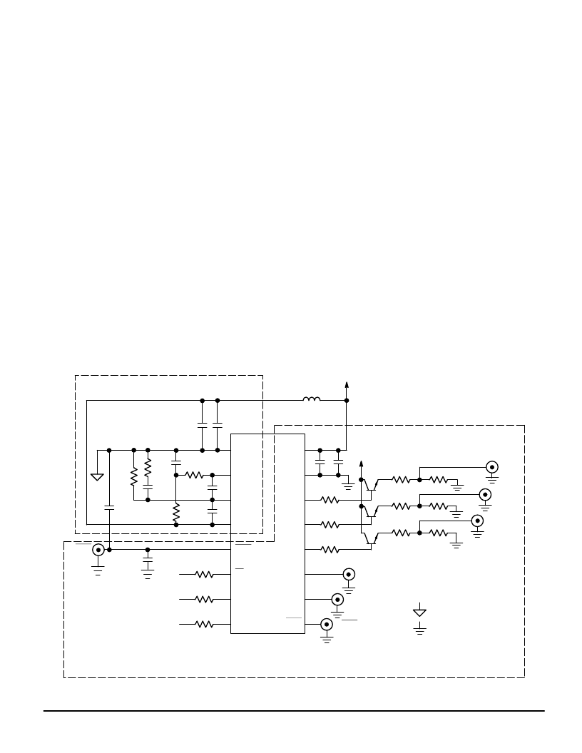
ing). Refer to the Application Diagram for the ground con-
nections.
The dc supply path for Pin 9 (VDD) should be separated
from other switching devices.
The LC filter should be connected between Pin 9 and Pin
4. Refer to the values used in the Application Diagram.
Biasing and filter networks should be connected to Pin 2
and Pin 3. Refer to the recommended networks in the Ap-
plication Diagram.
Two small capacitors can be connected between Pins 2
and 3, and between Pins 3 and 4.
Jittering
Most display jittering is caused by HFLB jittering on Pin 5.
Care must be taken if the HFLB signal comes from the fly-
back transformer. A short path and shielded cable are rec-
ommended for a clean signal. A small capacitor can be
added between Pin 5 and Pin 16 to smooth the signal. Refer
to the value used in the Application Diagram.
Display Dancing
Most display dancing is caused by interference of the seri-
al bus. It can be avoided by adding series resistors to the se-
rial bus.
APPLICATION DIAGRAM
MPS2369
100
μ
H
0.1
μ
F
100
μ
F
ANALOG GROUND – FLOATING
3.3 k
100
100
100
240
240
240
VCC
VCC
1 k
1 k
1 k
0.1
μ
F
10
μ
F
9
16
15
14
13
12
11
10
1
2
3
4
5
6
7
8
0.01
μ
F
2 k
0.047
μ
F
33 pF
33 pF
100
100
100
VDD
VSS
R
G
B
FBKG
HTONE
VFLB
VSS(A)
VCO
RP
HFLB
SS
SDA(MOSI)
SCL(SCK)
VDD(A)
HFLB
330 pF
2 k
VFLB
HTONE
FBKG
B
G
R
330 k
DIGITAL GROUND – COMMON GROUND
ANALOG GROUND
DIGITAL GROUND
AMOSD
IIC(SPI) BUS
330 pF
相關(guān)PDF資料 |
PDF描述 |
|---|---|
| MC141585 | Rad-Tolerant Class V, Floating Point Digital Signal Processor 429-CFCBGA -55 to 115 |
| MC14161B | SYNCHRONUS PRESETTABLE 4-BIT COUNTERS |
| MC14160BD | SYNCHRONUS PRESETTABLE 4-BIT COUNTERS |
| MC14160BL | SYNCHRONUS PRESETTABLE 4-BIT COUNTERS |
| MC14160B | Rad-Tolerant Class V, Floating Point Digital Signal Processor 429-CFCBGA -55 to 125 |
相關(guān)代理商/技術(shù)參數(shù) |
參數(shù)描述 |
|---|---|
| MC141555DW3 | 制造商:Rochester Electronics LLC 功能描述:- Bulk 制造商:Motorola Inc 功能描述: |
| MC141585DWE | 功能描述:IC LCD MONITOR OSD 16-SOIC RoHS:是 類別:集成電路 (IC) >> PMIC - 電源管理 - 專用 系列:- 應(yīng)用說明:Ultrasound Imaging Systems Application Note 產(chǎn)品培訓(xùn)模塊:Lead (SnPb) Finish for COTS Obsolescence Mitigation Program 標(biāo)準(zhǔn)包裝:37 系列:- 應(yīng)用:醫(yī)療用超聲波成像,聲納 電流 - 電源:- 電源電壓:2.37 V ~ 6 V 工作溫度:0°C ~ 70°C 安裝類型:表面貼裝 封裝/外殼:56-WFQFN 裸露焊盤 供應(yīng)商設(shè)備封裝:56-TQFN-EP(8x8) 包裝:管件 |
| MC141585DWER2 | 功能描述:IC LCD MONITOR OSD 16-SOIC RoHS:是 類別:集成電路 (IC) >> PMIC - 電源管理 - 專用 系列:- 應(yīng)用說明:Ultrasound Imaging Systems Application Note 產(chǎn)品培訓(xùn)模塊:Lead (SnPb) Finish for COTS Obsolescence Mitigation Program 標(biāo)準(zhǔn)包裝:37 系列:- 應(yīng)用:醫(yī)療用超聲波成像,聲納 電流 - 電源:- 電源電壓:2.37 V ~ 6 V 工作溫度:0°C ~ 70°C 安裝類型:表面貼裝 封裝/外殼:56-WFQFN 裸露焊盤 供應(yīng)商設(shè)備封裝:56-TQFN-EP(8x8) 包裝:管件 |
| MC14161BCPD | 制造商:Motorola Inc 功能描述: |
| MC14161BD | 制造商:Rochester Electronics LLC 功能描述:- Bulk |
發(fā)布緊急采購,3分鐘左右您將得到回復(fù)。