- 您現(xiàn)在的位置:買賣IC網(wǎng) > PDF目錄69020 > MB90F334APMC1 (FUJITSU LTD) 16-BIT, FLASH, 24 MHz, MICROCONTROLLER, PQFP120 PDF資料下載
參數(shù)資料
| 型號(hào): | MB90F334APMC1 |
| 廠商: | FUJITSU LTD |
| 元件分類: | 微控制器/微處理器 |
| 英文描述: | 16-BIT, FLASH, 24 MHz, MICROCONTROLLER, PQFP120 |
| 封裝: | 14 X 14 MM, 1.70 MM HEIGHT, 0.40 MM PITCH, PLASTIC, LFQFP-120 |
| 文件頁(yè)數(shù): | 3/72頁(yè) |
| 文件大小: | 1857K |
| 代理商: | MB90F334APMC1 |
第1頁(yè)第2頁(yè)當(dāng)前第3頁(yè)第4頁(yè)第5頁(yè)第6頁(yè)第7頁(yè)第8頁(yè)第9頁(yè)第10頁(yè)第11頁(yè)第12頁(yè)第13頁(yè)第14頁(yè)第15頁(yè)第16頁(yè)第17頁(yè)第18頁(yè)第19頁(yè)第20頁(yè)第21頁(yè)第22頁(yè)第23頁(yè)第24頁(yè)第25頁(yè)第26頁(yè)第27頁(yè)第28頁(yè)第29頁(yè)第30頁(yè)第31頁(yè)第32頁(yè)第33頁(yè)第34頁(yè)第35頁(yè)第36頁(yè)第37頁(yè)第38頁(yè)第39頁(yè)第40頁(yè)第41頁(yè)第42頁(yè)第43頁(yè)第44頁(yè)第45頁(yè)第46頁(yè)第47頁(yè)第48頁(yè)第49頁(yè)第50頁(yè)第51頁(yè)第52頁(yè)第53頁(yè)第54頁(yè)第55頁(yè)第56頁(yè)第57頁(yè)第58頁(yè)第59頁(yè)第60頁(yè)第61頁(yè)第62頁(yè)第63頁(yè)第64頁(yè)第65頁(yè)第66頁(yè)第67頁(yè)第68頁(yè)第69頁(yè)第70頁(yè)第71頁(yè)第72頁(yè)
MB90330A Series
DS07-13734-9E
11
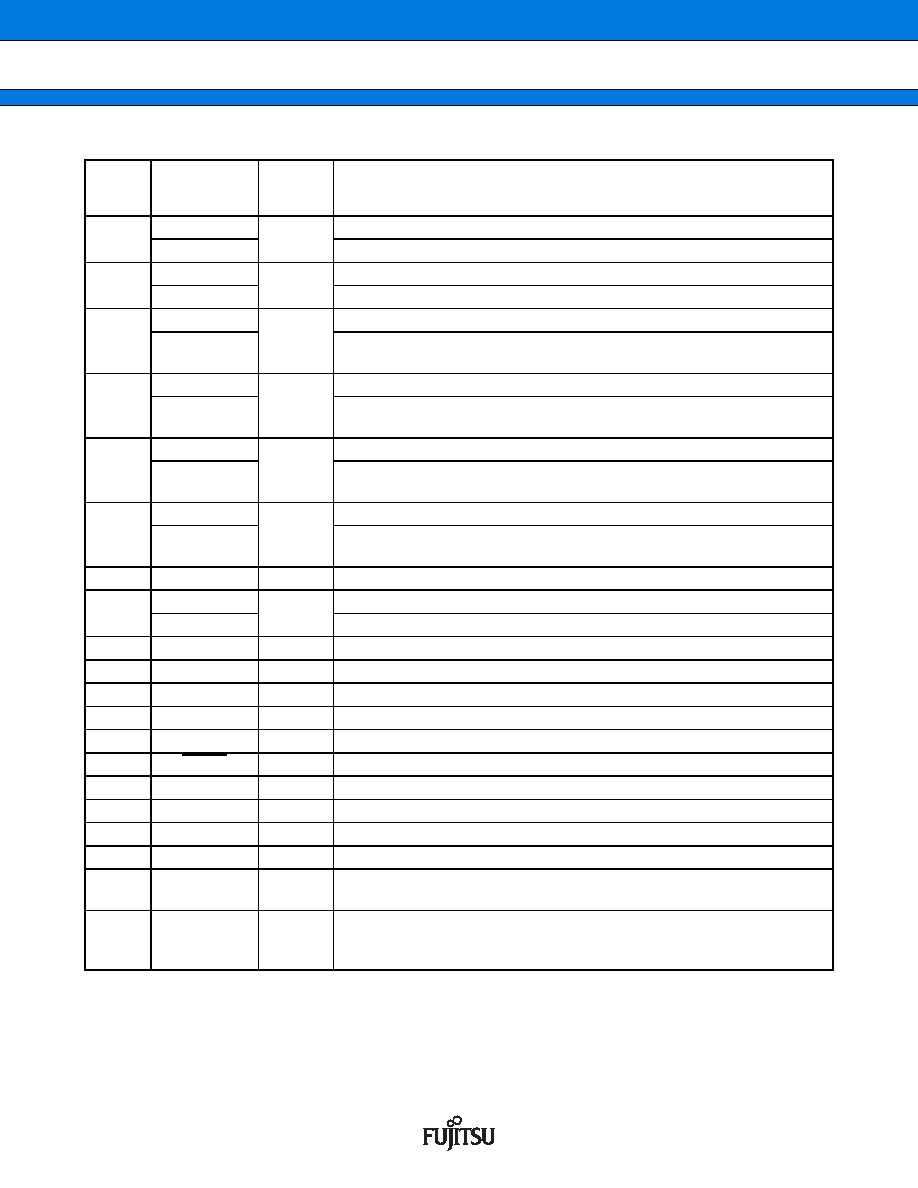
(Continued)
* : For circuit information, refer to “
■ I/O CIRCUIT TYPE”.
Pin no.
Pin name
I/O
Circuit
type*
Function
56 to 59
PA0 to PA3
C
General purpose input/output port. (Withstand voltage of 5 V)
IN0 to IN3
Function as the input capture ch.0 to ch.3 trigger inputs.
60 to 63
PA4 to PA7
C
General purpose input/output port. (Withstand voltage of 5 V)
OUT0 to OUT3
Function as the output compare ch.0 to ch.3 event output pins.
64
PB0
C
General purpose input/output port. (Withstand voltage of 5 V)
SCL1
Function as the ch.1 clock I/O pin for the I2C interface. Set port output to
High-Z during I2C interface operations.
65
PB1
C
General purpose input/output port. (Withstand voltage of 5 V)
SDA1
Function as the ch.1 data I/O pin for the I2C interface. Set port output to
High-Z during I2C interface operations.
66
PB2
C
General purpose input/output port. (Withstand voltage of 5 V)
SCL2
Function as the ch.2 clock I/O pin for the I2C interface. Set port output to
High-Z during I2C interface operations.
67
PB3
C
General purpose input/output port. (Withstand voltage of 5 V)
SDA2
Function as the ch.2 data I/O pin for the I2C interface. Set port output to
High-Z during I2C interface operations.
68
PB4
C
General purpose input/output port. (Withstand voltage of 5 V)
69, 70
PB5, PB6
D
General purpose input/output port.
PPG4, PPG5
Function as ch.4 and ch.5 output pins for the 8-bit PPG timer.
71
UTEST
C
USB test pin. Connect this to a pull-down resistor during normal usage.
73
DVM
K
USB function D
pin.
74
DVP
K
USB function D
+ pin.
77
HVM
K
USB HOST D
pin.
78
HVP
K
USB HOST D
+ pin.
80
HCON
E
External pull-up resistor connect pin.
36
AVcc
A/D converter power supply pin.
37
AVRH
J
A/D converter external reference power supply pin.
38
AVss
A/D converter power supply pin.
87 to 89
MD2 to MD0
B
Operation mode select input pin.
15, 75,
79, 105
Vcc
Power supply pin.
16, 47,
72, 76,
106
Vss
Power supply pin (GND).
相關(guān)PDF資料 |
PDF描述 |
|---|---|
| MB90F395HAPMT | 16-BIT, FLASH, 24 MHz, MICROCONTROLLER, PQFP120 |
| MB90F428GBPFV | 16-BIT, FLASH, 16 MHz, MICROCONTROLLER, PQFP100 |
| MB90F423GBPFV | 16-BIT, FLASH, 16 MHz, MICROCONTROLLER, PQFP100 |
| MB90423GBPFV | 16-BIT, MROM, 16 MHz, MICROCONTROLLER, PQFP100 |
| MB90427GBPFV | 16-BIT, MROM, 16 MHz, MICROCONTROLLER, PQFP100 |
相關(guān)代理商/技術(shù)參數(shù) |
參數(shù)描述 |
|---|---|
| MB90F334APMC1-GE1 | 制造商:FUJITSU 功能描述: |
| MB90F334APMC1-G-SPE1 | 制造商:FUJITSU 功能描述: |
| MB90F334APMC-G-JNE1 | 制造商:FUJITSU 功能描述: |
| MB90F334APMC-G-SNE1 | 制造商:FUJITSU 功能描述: |
| MB90F334APMC-G-SPE1 | 制造商:FUJITSU 功能描述: |
發(fā)布緊急采購(gòu),3分鐘左右您將得到回復(fù)。