- 您現(xiàn)在的位置:買賣IC網(wǎng) > PDF目錄377884 > MB8116400B-50 (Fujitsu Limited) 4 M ×4 BITS Fast Page Mode Dynamic RAM(CMOS 4 M ×4 位快速頁(yè)面存取模式RAM) PDF資料下載
參數(shù)資料
| 型號(hào): | MB8116400B-50 |
| 廠商: | Fujitsu Limited |
| 英文描述: | 4 M ×4 BITS Fast Page Mode Dynamic RAM(CMOS 4 M ×4 位快速頁(yè)面存取模式RAM) |
| 中文描述: | 4米× 4位快速頁(yè)面模式動(dòng)態(tài)RAM(的CMOS 4米× 4位快速頁(yè)面存取模式的RAM) |
| 文件頁(yè)數(shù): | 5/27頁(yè) |
| 文件大小: | 517K |
| 代理商: | MB8116400B-50 |
第1頁(yè)第2頁(yè)第3頁(yè)第4頁(yè)當(dāng)前第5頁(yè)第6頁(yè)第7頁(yè)第8頁(yè)第9頁(yè)第10頁(yè)第11頁(yè)第12頁(yè)第13頁(yè)第14頁(yè)第15頁(yè)第16頁(yè)第17頁(yè)第18頁(yè)第19頁(yè)第20頁(yè)第21頁(yè)第22頁(yè)第23頁(yè)第24頁(yè)第25頁(yè)第26頁(yè)第27頁(yè)
5
MB8116400B-50/-60
I
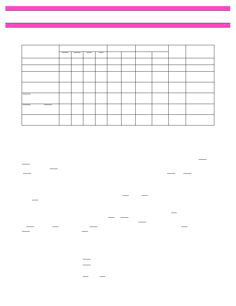
FUNCTIONAL TRUTH TABLE
X : “H” or “L”
* : It is impossible in Fast Page Mode.
I
ADDRESS INPUTS
Twenty-two input bits are required to decode any four of 16,777,216 cell addresses in the memory matrix. Since
only twelve address bits (A
0
to A
11
) are available, the row and column inputs are separately strobed by RAS and
CAS as shown in Figure 1. First, twelve row address bits are input on pins A
address strobe (RAS) then, ten column address bits are input and latched with the column address strobe
(CAS). Both row and column addresses must be stable on or before the falling edge of RAS and CAS, respectively.
The address latches are of the flow-through type; thus, address information appearing after t
matically treated as the column address.
WRITE ENABLE
The read or write mode is determined by the logic state of WE. When WE is active Low, a write cycle is initiated;
when WE is High, a read cycle is selected. During the read mode, input data is ignored.
DATA INPUT
Input data is written into memory in either of three basic ways–an early write cycle, an OE (delayed) write cycle,
and a read-modify-write cycle. The falling edge of WE or CAS, whichever is later, serves as the input data-latch
strobe. In an early write cycle, the input data (DQ
1
-DQ
4
) is strobed by CAS and the setup/hold times are referenced
to CAS because WE goes Low before CAS. In a delayed write or a read-modify-write cycle, WE goes Low after
CAS; thus, input data is strobed by WE and all setup/hold times are referenced to the write-enable signal.
DATA OUTPUT
The three-state buffers are TTL compatible with a fanout of two TTL loads. Polarity of the output data is identical to
that of the input; the output buffers remain in the high-impedance state until the column address strobe goes Low.
When a read or read-modify-write cycle is executed, valid outputs are obtained under the following conditions:
t
RAC
:
from the falling edge of RAS when t
RCD
(max) is satisfied.
t
CAC
:
from the falling edge of CAS when t
RCD
is greater than t
t
AA
:
from column address input when t
RAD
is greater than t
t
OEA
:
from the falling edge of OE when OE is brought Low after t
FUNCTIONAL OPERATION
0
-through-A
11
and latched with the row
RAH
(min)+ t
T
is auto-
RCD
(max).
(max).
RAD
RAC
, t
CAC
, or t
AA
.
Operation Mode
Clock Input
Address Input
Input Data
Refresh
Note
RAS
CAS
WE
OE
Row
Column
Input
Output
Standby
H
H
X
X
—
—
—
High-Z
—
Read Cycle
L
L
H
L
Valid
Valid
—
Valid
Yes*
t
RCS
≥
t
RCS
(min)
Write Cycle
(Early Write)
L
L
L
X
Valid
Valid
Valid
High-Z
Yes*
t
WCS
≥
t
WCS
(min)
Read-Modify-
Write Cycle
L
L
H
→
L L
→
H
Valid
Valid
Valid
Valid
Yes*
RAS-only
Refresh Cycle
L
H
X
X
Valid
—
—
High-Z
Yes
CAS-before-RAS
Refresh Cycle
L
L
H
X
—
—
—
High-Z
Yes
t
CSR
≥
t
CSR
(min)
Hidden Refresh
Cycle
H
→
L
L
H
→
X
L
—
—
—
Valid
Yes
Previous data
is kept.
相關(guān)PDF資料 |
PDF描述 |
|---|---|
| MB8116400B-60 | 4 M ×4 BITS Fast Page Mode Dynamic RAM(CMOS 4 M ×4 位快速頁(yè)面存取模式RAM) |
| MB8116405A-60 | CMOS 4M ×4 BIT Hyper Page Mode Dynamic RAM(CMOS 4M ×4 位超級(jí)頁(yè)面存取模式動(dòng)態(tài)RAM) |
| MB8116405A-70 | CMOS 4M ×4 BIT Hyper Page Mode Dynamic RAM(CMOS 4M ×4 位超級(jí)頁(yè)面存取模式動(dòng)態(tài)RAM) |
| MB81164442A-100L | CMOS 4×4M×16 BIT Synchronous Dynamic Random Access Memory (SDRAM)(CMOS 4×4M×16 位同步動(dòng)態(tài)RAM) |
| MB81164442A-100 | CMOS 4×4M×16 BIT Synchronous Dynamic Random Access Memory (SDRAM)(CMOS 4×4M×16 位同步動(dòng)態(tài)RAM) |
相關(guān)代理商/技術(shù)參數(shù) |
參數(shù)描述 |
|---|---|
| MB8116E | 制造商:FUJITSU 功能描述: 制造商:FUJITSU 功能描述:8116E |
| MB8117800A-60 | 制造商:未知廠家 制造商全稱:未知廠家 功能描述:2 M X 8 BIT FAST PAGE MODE DYNAMIC RAM |
| MB8117800A-70 | 制造商:未知廠家 制造商全稱:未知廠家 功能描述:2 M X 8 BIT FAST PAGE MODE DYNAMIC RAM |
| MB812 | 功能描述:ACCY MOUNT BMM 3/4 58A RoHS:是 類別:RF/IF 和 RFID >> RF配件 系列:* 標(biāo)準(zhǔn)包裝:1 系列:* |
| MB812.833 | 功能描述:ACCY MOUNT BMM 3/4 58A RoHS:是 類別:RF/IF 和 RFID >> RF配件 系列:* 標(biāo)準(zhǔn)包裝:1 系列:* |
發(fā)布緊急采購(gòu),3分鐘左右您將得到回復(fù)。