- 您現(xiàn)在的位置:買賣IC網(wǎng) > PDF目錄377882 > MB582A (Fujitsu Limited) 155-Mbps ATM Transceiver(155Mbps 異步傳輸模式 收發(fā)器) PDF資料下載
參數(shù)資料
| 型號: | MB582A |
| 廠商: | Fujitsu Limited |
| 英文描述: | 155-Mbps ATM Transceiver(155Mbps 異步傳輸模式 收發(fā)器) |
| 中文描述: | 155 - Mbps的自動柜員機收發(fā)器(155Mbps異步傳輸模式收發(fā)器) |
| 文件頁數(shù): | 42/46頁 |
| 文件大?。?/td> | 345K |
| 代理商: | MB582A |
第1頁第2頁第3頁第4頁第5頁第6頁第7頁第8頁第9頁第10頁第11頁第12頁第13頁第14頁第15頁第16頁第17頁第18頁第19頁第20頁第21頁第22頁第23頁第24頁第25頁第26頁第27頁第28頁第29頁第30頁第31頁第32頁第33頁第34頁第35頁第36頁第37頁第38頁第39頁第40頁第41頁當前第42頁第43頁第44頁第45頁第46頁
42
MB582A/583A
I
PRECAUTIONS
(1) For the V
CC
supplied to the MB582A/583A, use a stable power supply. If spike noise enters the power supply,
the MB582A/583A may fail to perform stable operation.
1-1. The power supply for this LSI should be separated from the power supply for any other LSI not to receive
digital noise (as shown in the following illustration).
1-2. To prevent spike noise from another LSIs, add sufficient capacitance also to another LSIs (for example, 10
μ
F for each of the LSIs).
1-3. Connect a bypass capacitor of about 0.1
μ
F closer (as within 10 mm as possible) to the pins between each
V
CC
and GND.
Between AV
CC
and AGND which are an analog V
CC
and an analog GND, in particular, connect a bypass
capacitor closer (within 10 mm) to the LSI pins.
For the power source, attach a capacitor with a large value of about 10
μ
F to provide stable power.
(2) A external filter capacitor between FIL1 and FIL2 must be placed closer (as within 15 mm as possible) to the
LSI pins. This capacitor must be wired by minimum routing. The wiring should not cross any other pattern.
The pins are particularly sensitive to external noise. Placing this capacitor at lower-noise positions ensure their
stable operations. In addition, routing GND patterns around the pins and the capacitor greatly contributes to
stable operation.
(3) Letting the wiring for reference clock signals supplied to the REFCLK and PICLK cross other patterns increases
jitter, leading to unstable operation.
Note also that input of a reference clock signal with large undershoot results in unstable operation.
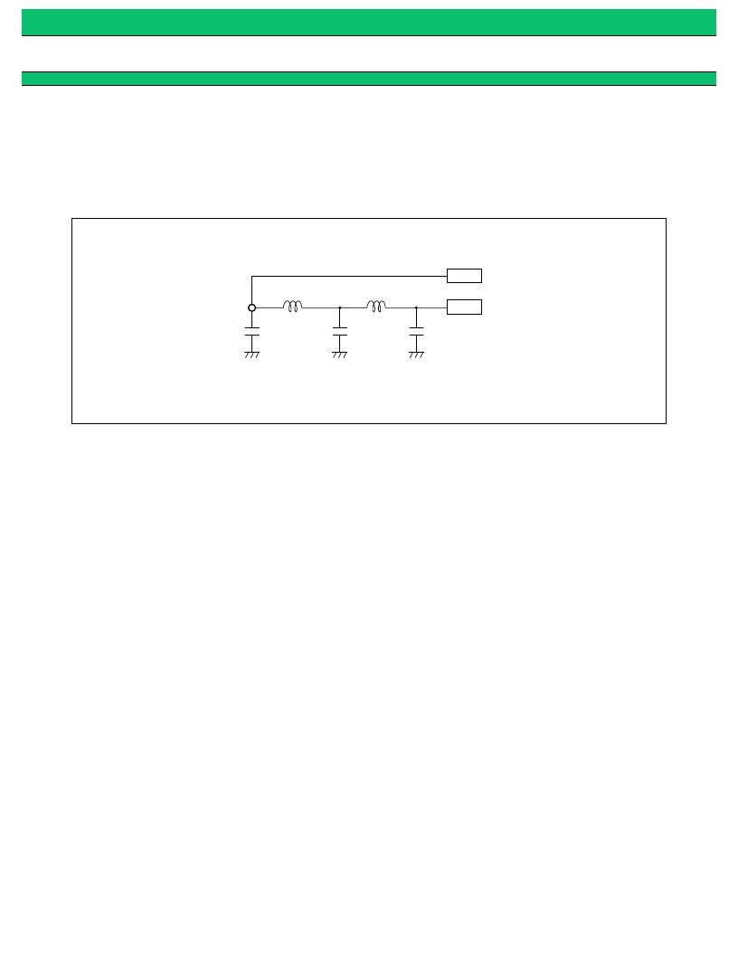
Board V
CC
pin
10
μ
F or more
10
μ
F or more
4.7
μ
H or more
4.7
μ
H or more
Another logic LSI’s V
CC
pattern
Transceiver’s V
CC
pattern
Connection example
10
μ
F or more
Note: Suppress the total voltage drop by the inductor to be 50 mV or less.
(Inductor allowable current = 0.5 A or more; Inductor total DC resistance = 0.1
or less)
相關(guān)PDF資料 |
PDF描述 |
|---|---|
| MB6021A | PCM Coders/Decoders(脈沖編碼器/解碼器) |
| MB60HXXX | CMOS Gate Array |
| MB61VHXXX | CMOS Gate Array |
| MB63HXXX | CMOS Gate Array |
| MB64HBXXX | CMOS Gate Array |
相關(guān)代理商/技術(shù)參數(shù) |
參數(shù)描述 |
|---|---|
| MB59 | 制造商:PANJIT 制造商全稱:Pan Jit International Inc. 功能描述:SURFACE MOUNT SCHOTTKY BARRIER RECTIFIER |
| MB59101BAN | 制造商:MURATA 制造商全稱:Murata Manufacturing Co., Ltd. 功能描述:HIGH FREQUENCY CERAMIC CAPACITORS |
| MB59101BBN | 制造商:MURATA 制造商全稱:Murata Manufacturing Co., Ltd. 功能描述:HIGH FREQUENCY CERAMIC CAPACITORS |
| MB59101CAN | 制造商:MURATA 制造商全稱:Murata Manufacturing Co., Ltd. 功能描述:HIGH FREQUENCY CERAMIC CAPACITORS |
| MB59101CBN | 制造商:MURATA 制造商全稱:Murata Manufacturing Co., Ltd. 功能描述:HIGH FREQUENCY CERAMIC CAPACITORS |
發(fā)布緊急采購,3分鐘左右您將得到回復(fù)。