- 您現(xiàn)在的位置:買(mǎi)賣(mài)IC網(wǎng) > PDF目錄385556 > MAX9489ETJ (MAXIM INTEGRATED PRODUCTS INC) Multiple-Output Network Clock Generator PDF資料下載
參數(shù)資料
| 型號(hào): | MAX9489ETJ |
| 廠商: | MAXIM INTEGRATED PRODUCTS INC |
| 元件分類(lèi): | XO, clock |
| 英文描述: | Multiple-Output Network Clock Generator |
| 中文描述: | 133 MHz, OTHER CLOCK GENERATOR, QCC32 |
| 封裝: | 5 X 5 MM, 0.80 MM PITCH, TQFN-32 |
| 文件頁(yè)數(shù): | 8/11頁(yè) |
| 文件大?。?/td> | 176K |
| 代理商: | MAX9489ETJ |
M
Multiple-Output Network Clock Generator
8
_______________________________________________________________________________________
Writing to the MAX9489
Writing to the MAX9489 begins with a START condition
(Figures 3 and 4). Following the START condition, each
pulse on SCL transfers 1 bit of data. The first 7 bits
comprise the device address (see the
Device Address
section). The 8th bit is low to indicate a write operation.
An acknowledge bit is then generated by the
MAX9489, signaling that it recognizes its address. The
next 8 bits form the register address byte (Table 2) and
determine which control register will receive the follow-
ing data byte. The MAX9489 then generates another
acknowledge bit. The data byte is then written into the
addressed register of the MAX9489. An acknowledge
bit by the MAX9489 followed by a required STOP con-
dition by the master complete the communication. To
write to the device again, repeat the entire write proce-
dure; I
2
C burst write mode is not supported by the
MAX9489.
Reading the MAX9489 Setup
Reading from the MAX9489 registers begins with a
START condition and a device address with the write
bit set low, then the register address that is to be read,
followed by a repeated START condition and a device
address with the write bit set high, and finally the data
are shifted out (Figure 4). Following a START condition,
the first 7 bits comprise the device address. The 8th bit
is low to indicate a write operation (to write in the
following register address). An acknowledge bit is
then generated by the MAX9489, signaling that it re-
cognizes its address. The next 8 bits form the register
address, indicating the location of the data to be read,
followed by another acknowledge, again generated by
the MAX9489. The master then produces a repeated
START condition and readdresses the device, this time
with the R/
W
bit high to indicate a read operation
(Figure 4). The MAX9489 generates an acknowledge
bit, signaling that it recognizes its address. The data
byte is then clocked out of the MAX9489. A final not-
acknowledge bit, generated by the master (not
required), and a STOP condition, also generated by the
master, complete the communication. To read from the
device again, the entire read procedure is repeated;
I
2
C burst read mode is not supported by the MAX9489.
Device Control Registers
The MAX9489 has 17 control registers. The register
addresses and functions are shown in Table 2. The first
16 registers are used to set the 15 outputs, with register
0x00 controlling all outputs simultaneously and the rest
mapped to individual outputs. Register 0x10 accesses
the frequency-margin control. All other addresses are
reserved and are not to be used.
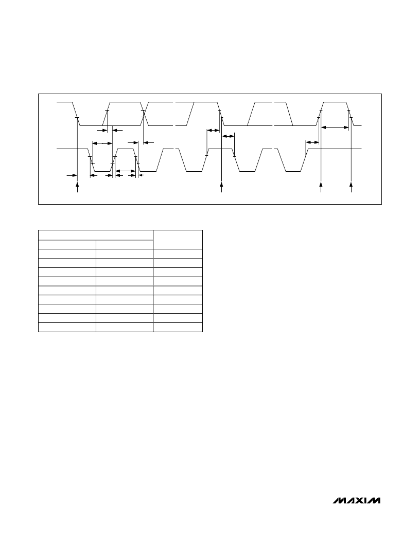
SCL
SDA
START CONDITION
STOP CONDITION
REPEATED START CONDITION
START CONDITION
t
SU, DAT
t
HD, DAT
t
LOW
t
HD, STA
t
HIGH
t
R
t
F
t
SU, STA
t
HD, STA
t
SU, STO
t
BUF
Figure 2. Serial Interface Timing
PIN
SA1
Open
Open
Open
GND
GND
GND
V
DD
V
DD
V
DD
SA0
V
DD
GND
Open
V
DD
GND
Open
V
DD
GND
Open
DEVICE
ADDRESS
110 0010
110 0100
110 1000
111 0000
110 1001
110 1100
111 0100
111 0010
111 0001
Table 1. Device I
2
C Address Selection
相關(guān)PDF資料 |
PDF描述 |
|---|---|
| MAX9491ETP | Factory-Programmable, Single PLL Clock Generator |
| MAX9491EUD | Factory-Programmable, Single PLL Clock Generator |
| MAX9491 | Factory-Programmable, Single PLL Clock Generator |
| MAX9492 | Multiple-Output Clock Generator with Spread Spectrum |
| MAX9492ETP | Multiple-Output Clock Generator with Spread Spectrum |
相關(guān)代理商/技術(shù)參數(shù) |
參數(shù)描述 |
|---|---|
| MAX9491ETP010 | 功能描述:時(shí)鐘發(fā)生器及支持產(chǎn)品 RoHS:否 制造商:Silicon Labs 類(lèi)型:Clock Generators 最大輸入頻率:14.318 MHz 最大輸出頻率:166 MHz 輸出端數(shù)量:16 占空比 - 最大:55 % 工作電源電壓:3.3 V 工作電源電流:1 mA 最大工作溫度:+ 85 C 安裝風(fēng)格:SMD/SMT 封裝 / 箱體:QFN-56 |
| MAX9491ETP010+ | 功能描述:時(shí)鐘發(fā)生器及支持產(chǎn)品 Factory-Prog Single PLL Clock Generator RoHS:否 制造商:Silicon Labs 類(lèi)型:Clock Generators 最大輸入頻率:14.318 MHz 最大輸出頻率:166 MHz 輸出端數(shù)量:16 占空比 - 最大:55 % 工作電源電壓:3.3 V 工作電源電流:1 mA 最大工作溫度:+ 85 C 安裝風(fēng)格:SMD/SMT 封裝 / 箱體:QFN-56 |
| MAX9491ETP010+T | 功能描述:時(shí)鐘發(fā)生器及支持產(chǎn)品 Factory-Prog Single PLL Clock Generator RoHS:否 制造商:Silicon Labs 類(lèi)型:Clock Generators 最大輸入頻率:14.318 MHz 最大輸出頻率:166 MHz 輸出端數(shù)量:16 占空比 - 最大:55 % 工作電源電壓:3.3 V 工作電源電流:1 mA 最大工作溫度:+ 85 C 安裝風(fēng)格:SMD/SMT 封裝 / 箱體:QFN-56 |
| MAX9491ETP010-T | 功能描述:時(shí)鐘發(fā)生器及支持產(chǎn)品 RoHS:否 制造商:Silicon Labs 類(lèi)型:Clock Generators 最大輸入頻率:14.318 MHz 最大輸出頻率:166 MHz 輸出端數(shù)量:16 占空比 - 最大:55 % 工作電源電壓:3.3 V 工作電源電流:1 mA 最大工作溫度:+ 85 C 安裝風(fēng)格:SMD/SMT 封裝 / 箱體:QFN-56 |
| MAX9491ETP045 | 功能描述:時(shí)鐘發(fā)生器及支持產(chǎn)品 RoHS:否 制造商:Silicon Labs 類(lèi)型:Clock Generators 最大輸入頻率:14.318 MHz 最大輸出頻率:166 MHz 輸出端數(shù)量:16 占空比 - 最大:55 % 工作電源電壓:3.3 V 工作電源電流:1 mA 最大工作溫度:+ 85 C 安裝風(fēng)格:SMD/SMT 封裝 / 箱體:QFN-56 |
發(fā)布緊急采購(gòu),3分鐘左右您將得到回復(fù)。