- 您現(xiàn)在的位置:買賣IC網(wǎng) > PDF目錄11564 > MAX3421EETJ+T (Maxim Integrated Products)IC USB PERIPH/HOST CNTRL 32TQFN PDF資料下載
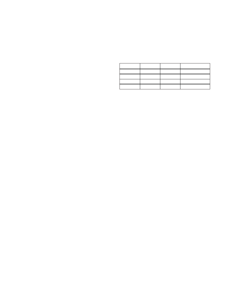
參數(shù)資料
| 型號(hào): | MAX3421EETJ+T |
| 廠商: | Maxim Integrated Products |
| 文件頁(yè)數(shù): | 8/28頁(yè) |
| 文件大小: | 0K |
| 描述: | IC USB PERIPH/HOST CNTRL 32TQFN |
| 產(chǎn)品培訓(xùn)模塊: | Lead (SnPb) Finish for COTS Obsolescence Mitigation Program |
| 標(biāo)準(zhǔn)包裝: | 2,500 |
| 控制器類型: | USB 外設(shè)控制器 |
| 接口: | USB/串行 |
| 電源電壓: | 3 V ~ 3.6 V |
| 電流 - 電源: | 15mA |
| 工作溫度: | -40°C ~ 85°C |
| 安裝類型: | 表面貼裝 |
| 封裝/外殼: | 32-WFQFN 裸露焊盤(pán) |
| 供應(yīng)商設(shè)備封裝: | 32-TQFN-EP(5x5) |
| 包裝: | 帶卷 (TR) |
| 配用: | MAX3421EVKIT-1+-ND - EVAL KIT FOR MAX3421E |
第1頁(yè)第2頁(yè)第3頁(yè)第4頁(yè)第5頁(yè)第6頁(yè)第7頁(yè)當(dāng)前第8頁(yè)第9頁(yè)第10頁(yè)第11頁(yè)第12頁(yè)第13頁(yè)第14頁(yè)第15頁(yè)第16頁(yè)第17頁(yè)第18頁(yè)第19頁(yè)第20頁(yè)第21頁(yè)第22頁(yè)第23頁(yè)第24頁(yè)第25頁(yè)第26頁(yè)第27頁(yè)第28頁(yè)
MAX3421E
USB Peripheral/Host Controller
with SPI Interface
16
Maxim Integrated
help sustain bandwidth by allowing data to move concur-
rently over USB and the SPI interface.
VCC
Power the USB transceiver and digital logic by apply-
ing a positive 3.3V supply to VCC. Bypass VCC to GND
with a 1.0F ceramic capacitor as close to the VCC pin
as possible.
VL
VL acts as a reference level for the SPI interface and all
other digital inputs and outputs. Connect VL to the sys-
tem’s logic-level power supply. Internal level translators
and VL allow the SPI interface and all general-purpose
inputs and outputs to operate at a system voltage
between 1.4V and 3.6V.
The MAX3421E features a USB VBUS detector input,
VBCOMP. The VBCOMP pin can withstand input volt-
ages up to 6V. Bypass VBCOMP to GND with a 1.0F
ceramic capacitor. VBCOMP is internally connected to
a voltage comparator to allow the SPI master to detect
(through an interrupt or checking a register bit) the
presence or loss of power on VBUS. VBCOMP does not
power any internal circuitry inside the MAX3421E.
VBCOMP is pulled down to ground with RIN (see
Electrical Characteristics).
VBCOMP in Peripheral Mode
VBCOMP is internally connected to a voltage compara-
tor so that the SPI master can detect the presence or
absence of VBUS. According to the USB 2.0 specifica-
tion, a self-powered peripheral must disconnect its
1.5k
Ω pullup resistor to D+ in the event that the host
turns off bus power. The VBGATE bit in the USBCTL
(R15) register provides the option for the MAX3421E
internal logic to automatically disconnect the 1.5k
Ω
resistor on D+. The VBGATE and CONNECT bits of
USBCTL (R15), along with the VBCOMP comparator
output (VBUS_DET), control the pullup resistor between
VCC and D+ as shown in Table 3 and the Functional
Diagram. Note that if VBGATE = 1 and VBUS_DET = 0,
the pullup resistor is disconnected regardless of the
CONNECT bit setting. If the device using the
MAX3421E is bus powered (through a +3.3V regulator
connected to VCC), the MAX3421E VBCOMP input can
be used as a general-purpose input. See the
Applications Information section for more details about
this connection.
VBCOMP in Host Mode
When using the MAX3421E in host mode, the presence
of VBUS does not need to be detected. In this case, the
VBCOMP input can be used as a general-purpose
input.
D+ and D-
The internal USB full-/low-speed transceiver is brought
out to the bidirectional data pins D+ and D-. These pins
are ±15kV ESD protected. Connect D+ and D- to a
USB B connector through 33
Ω ±1% series resistors.
D+ and D- in Peripheral Mode
In peripheral mode, the D+ and D- pins connect to a
USB B connector through series resistors. A switchable
1.5k
Ω pullup resistor is internally connected to D+.
D+ and D- in Host Mode
In host mode, the D+ and D- pins connect to a USB A
connector through series resistors. Switchable 15k
Ω
pulldown resistors are internally connected to D+ and
D-. The DPPULLDN and DMPULLDN bits in the MODE
(R27) register control the connection between D+ and
D- to GND. For host operation, set these bits to 1 to
enable the pulldown resistors. A host interrupt bit called
CONNIRQ alerts the SPI master when a peripheral is
attached or detached.
XI and XO
XI and XO connect an external 12MHz crystal to the
internal oscillator circuit. XI is the crystal oscillator
input, and XO is the crystal oscillator output. Connect
one side of a 12MHz
±0.25% parallel resonant crystal
to XI, and connect XO to the other side. Connect load
capacitors (20pF max) to ground on both XI and XO. XI
can also be driven with an external 12MHz ±0.25%
clock. If driving XI with an external clock, leave XO
unconnected. The external clock must meet the voltage
characteristics depicted in the
Electrical Character-
istics table. Internal logic is single-edge triggered. The
external clock should have a nominal 50% duty cycle.
Table 3. Internal Pullup Resistor Control
in Peripheral Mode
CONNECT
VBGATE
VBUS_DET
PULLUP
0
X
Not Connected
1
0
X
Connected
1
0
Not Connected
1
Connected
相關(guān)PDF資料 |
PDF描述 |
|---|---|
| V375C28M75B3 | CONVERTER MOD DC/DC 28V 75W |
| MAX5942BESE+ | IC IEEE 802.3AF POE SYSTM 16SOIC |
| 78Q8430-100IGTR/F | IC LAN MEDIA ACCESS CTLR 100LQFP |
| GRM2165C1H510JZ01D | CAP CER 51PF 50V 5% NP0 0805 |
| MAX5942BCSE+ | IC IEEE 802.3AF POE SYSTM 16SOIC |
相關(guān)代理商/技術(shù)參數(shù) |
參數(shù)描述 |
|---|---|
| MAX3421EVKIT-1+ | 功能描述:界面開(kāi)發(fā)工具 MAX3421E/20E Eval Kit RoHS:否 制造商:Bourns 產(chǎn)品:Evaluation Boards 類型:RS-485 工具用于評(píng)估:ADM3485E 接口類型:RS-485 工作電源電壓:3.3 V |
| MAX3430CPA | 功能描述:RS-485接口IC RoHS:否 制造商:Texas Instruments 數(shù)據(jù)速率:250 Kbps 工作電源電壓:3.3 V 電源電流:750 uA 工作溫度范圍:- 40 C to + 125 C 安裝風(fēng)格:SMD/SMT 封裝 / 箱體:SOIC-8 封裝:Tube |
| MAX3430CPA+ | 功能描述:RS-485接口IC Fail-Safe 1/4-Unit 3.3V Transceiver RoHS:否 制造商:Texas Instruments 數(shù)據(jù)速率:250 Kbps 工作電源電壓:3.3 V 電源電流:750 uA 工作溫度范圍:- 40 C to + 125 C 安裝風(fēng)格:SMD/SMT 封裝 / 箱體:SOIC-8 封裝:Tube |
| MAX3430CSA | 功能描述:RS-485接口IC RoHS:否 制造商:Texas Instruments 數(shù)據(jù)速率:250 Kbps 工作電源電壓:3.3 V 電源電流:750 uA 工作溫度范圍:- 40 C to + 125 C 安裝風(fēng)格:SMD/SMT 封裝 / 箱體:SOIC-8 封裝:Tube |
| MAX3430CSA+ | 功能描述:RS-485接口IC Fail-Safe 1/4-Unit 3.3V Transceiver RoHS:否 制造商:Texas Instruments 數(shù)據(jù)速率:250 Kbps 工作電源電壓:3.3 V 電源電流:750 uA 工作溫度范圍:- 40 C to + 125 C 安裝風(fēng)格:SMD/SMT 封裝 / 箱體:SOIC-8 封裝:Tube |
發(fā)布緊急采購(gòu),3分鐘左右您將得到回復(fù)。