- 您現(xiàn)在的位置:買賣IC網(wǎng) > PDF目錄383312 > MAX1191ETI-T (MAXIM INTEGRATED PRODUCTS INC) Ultra-Low-Power, 7.5Msps, Dual 8-Bit ADC PDF資料下載
參數(shù)資料
| 型號: | MAX1191ETI-T |
| 廠商: | MAXIM INTEGRATED PRODUCTS INC |
| 元件分類: | ADC |
| 英文描述: | Ultra-Low-Power, 7.5Msps, Dual 8-Bit ADC |
| 中文描述: | 2-CH 8-BIT FLASH METHOD ADC, PARALLEL ACCESS, QCC28 |
| 封裝: | 5 X 5 MM, 0.80 MM HEIGHT, MO-220, TQFN-28 |
| 文件頁數(shù): | 16/27頁 |
| 文件大?。?/td> | 492K |
| 代理商: | MAX1191ETI-T |
第1頁第2頁第3頁第4頁第5頁第6頁第7頁第8頁第9頁第10頁第11頁第12頁第13頁第14頁第15頁當(dāng)前第16頁第17頁第18頁第19頁第20頁第21頁第22頁第23頁第24頁第25頁第26頁第27頁
M
Ultra-Low-Power, 7.5Msps, Dual 8-Bit ADC
16
______________________________________________________________________________________
values originally held on C2a and C2b. These values
are then presented to the first stage quantizers and iso-
late the pipelines from the fast-changing inputs. The
wide input bandwidth T/H amplifiers allow the MAX1191
to track and sample/hold analog inputs of high frequen-
cies (>Nyquist). Both ADC inputs (INA+, INB+, INA-,
and INB-) can be driven either differentially or single
ended. Match the impedance of INA+ and INA-, as well
as INB+ and INB-, and set the common-mode voltage
to midsupply (V
DD
/2) for optimum performance.
Analog Inputs and Reference
Configurations
The MAX1191 full-scale analog input range is ±V
REF
with a common-mode input range of V
DD
/2 ±0.2V. V
REF
is the difference between V
REFP
and V
REFN
. The
MAX1191 provides three modes of reference operation.
The voltage at REFIN (V
REFIN
) sets the reference oper-
ation mode (Table 1).
In internal reference mode, connect REFIN to V
DD
or
leave REFIN unconnected. V
REF
is internally generated
to be 0.512V ±3%. COM, REFP, and REFN are low-
impedance outputs with V
COM
= V
DD
/2, V
REFP
= V
DD
/2
+ V
REF
/2, and V
REFN
= V
DD
/2 - V
REF
/2. Bypass REFP,
REFN, and COM each with a 0.33μF capacitor.
In buffered external reference mode, apply a 1.024V
±10% at REFIN. In this mode, COM, REFP, and REFN
are low-impedance outputs with V
COM
= V
DD
/2, V
REFP
=
V
DD
/2 + V
REFIN
/4, and V
REFN
= V
DD
/2 - V
REFIN
/4.
Bypass REFP, REFN, and COM each with a 0.33μF
capacitor. Bypass REFIN to GND with a 0.1μF capacitor.
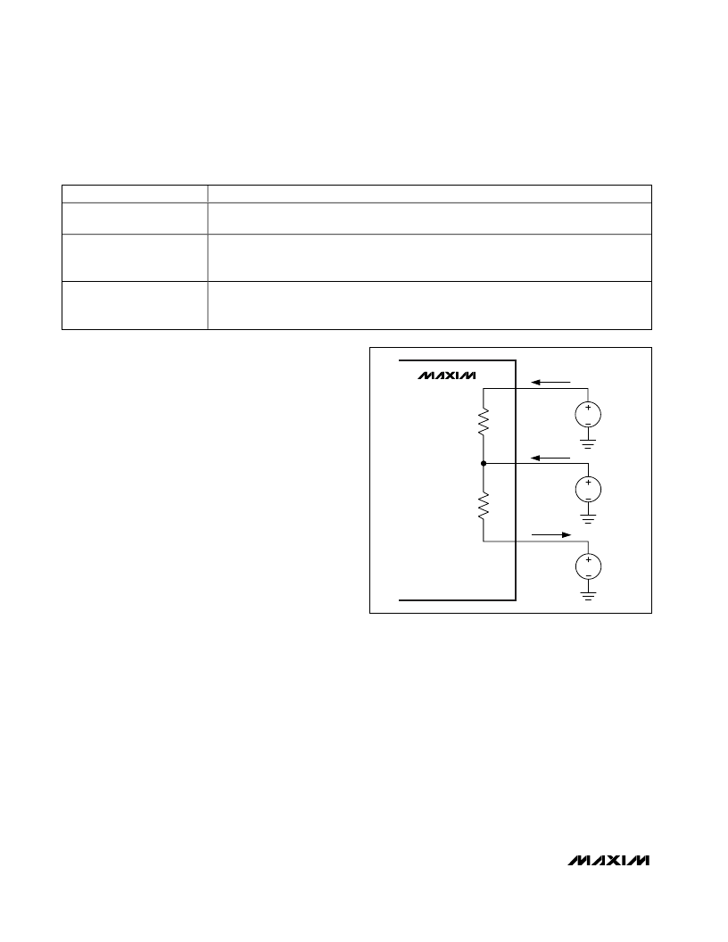
In unbuffered external reference mode, connect REFIN
to GND. This deactivates the on-chip reference buffers
for COM, REFP, and REFN. With their buffers shut
down, these nodes become high-impedance inputs
(
Figure
4) and can be driven through separate, external
reference sources. Drive V
COM
to V
DD
/2 ±10%, drive
V
REFP
to (V
DD
/2 +0.256V) ±10%, and drive V
REFN
to
(V
DD
/2 - 0.256V) ±10%. Bypass REFP, REFN, and COM
each with a 0.33μF capacitor.
For detailed circuit suggestions and how to drive this
dual ADC in buffered/unbuffered external reference
mode, see the
Applications Information
section.
Clock Input (CLK)
CLK accepts a CMOS-compatible signal level. Since
the interstage conversion of the device depends on the
repeatability of the rising and falling edges of the exter-
nal clock, use a clock with low jitter and fast rise and
fall times (<2ns). In particular, sampling occurs on the
rising edge of the clock signal, requiring this edge to
Figure 4. Unbuffered External Reference Mode Impedance
V
REFIN
REFERENCE MODE
>0.8 x V
DD
Internal reference mode. V
REF
is internally generated to be 0.512V. Bypass REFP, REFN, and COM
each with a 0.33μF capacitor.
1.024V ±10%
Buffered external reference mode. An external 1.024V ±10% reference voltage is applied to
REFIN. V
REF
is internally generated to be V
REFIN
/2. Bypass REFP, REFN, and COM each with a
0.33μF capacitor. Bypass REFIN to GND with a 0.1μF capacitor.
<0.3V
Unbuffered external reference mode. REFP, REFN, and COM are driven by external reference
sources. V
REF
is the difference between the externally applied V
REFP
and V
REFN
. Bypass REFP,
REFN, and COM each with a 0.33μF capacitor.
Table 1. Reference Modes
MAX1191
1.5V
1.25V
1.75V
62.5
μ
A
0
μ
A
COM
REFN
REFP
4k
4k
62.5
μ
A
相關(guān)PDF資料 |
PDF描述 |
|---|---|
| MAX1198 | Dual, 8-Bit, 100Msps, 3.3V, Low-Power ADC with Internal Reference and Parallel Outputs |
| MAX1198ECM | Dual, 8-Bit, 100Msps, 3.3V, Low-Power ADC with Internal Reference and Parallel Outputs |
| MAX1200 | +5v sINGLE-sUPPLY, 1mSPS, 16-bIT sELF-cALIBRATING adc |
| MAX1200AEMH | +5v sINGLE-sUPPLY, 1mSPS, 16-bIT sELF-cALIBRATING adc |
| MAX1200BCMH | +5v sINGLE-sUPPLY, 1mSPS, 16-bIT sELF-cALIBRATING adc |
相關(guān)代理商/技術(shù)參數(shù) |
參數(shù)描述 |
|---|---|
| MAX1192ETI | 功能描述:模數(shù)轉(zhuǎn)換器 - ADC RoHS:否 制造商:Texas Instruments 通道數(shù)量:2 結(jié)構(gòu):Sigma-Delta 轉(zhuǎn)換速率:125 SPs to 8 KSPs 分辨率:24 bit 輸入類型:Differential 信噪比:107 dB 接口類型:SPI 工作電源電壓:1.7 V to 3.6 V, 2.7 V to 5.25 V 最大工作溫度:+ 85 C 安裝風(fēng)格:SMD/SMT 封裝 / 箱體:VQFN-32 |
| MAX1192ETI+ | 功能描述:模數(shù)轉(zhuǎn)換器 - ADC 8-Bit 2Ch 22Msps 3.6V Precision ADC RoHS:否 制造商:Texas Instruments 通道數(shù)量:2 結(jié)構(gòu):Sigma-Delta 轉(zhuǎn)換速率:125 SPs to 8 KSPs 分辨率:24 bit 輸入類型:Differential 信噪比:107 dB 接口類型:SPI 工作電源電壓:1.7 V to 3.6 V, 2.7 V to 5.25 V 最大工作溫度:+ 85 C 安裝風(fēng)格:SMD/SMT 封裝 / 箱體:VQFN-32 |
| MAX1192ETI+T | 功能描述:模數(shù)轉(zhuǎn)換器 - ADC 8-Bit 2Ch 22Msps 3.6V Precision ADC RoHS:否 制造商:Texas Instruments 通道數(shù)量:2 結(jié)構(gòu):Sigma-Delta 轉(zhuǎn)換速率:125 SPs to 8 KSPs 分辨率:24 bit 輸入類型:Differential 信噪比:107 dB 接口類型:SPI 工作電源電壓:1.7 V to 3.6 V, 2.7 V to 5.25 V 最大工作溫度:+ 85 C 安裝風(fēng)格:SMD/SMT 封裝 / 箱體:VQFN-32 |
| MAX1192ETI-T | 功能描述:模數(shù)轉(zhuǎn)換器 - ADC RoHS:否 制造商:Texas Instruments 通道數(shù)量:2 結(jié)構(gòu):Sigma-Delta 轉(zhuǎn)換速率:125 SPs to 8 KSPs 分辨率:24 bit 輸入類型:Differential 信噪比:107 dB 接口類型:SPI 工作電源電壓:1.7 V to 3.6 V, 2.7 V to 5.25 V 最大工作溫度:+ 85 C 安裝風(fēng)格:SMD/SMT 封裝 / 箱體:VQFN-32 |
| MAX1193ETI | 功能描述:模數(shù)轉(zhuǎn)換器 - ADC RoHS:否 制造商:Texas Instruments 通道數(shù)量:2 結(jié)構(gòu):Sigma-Delta 轉(zhuǎn)換速率:125 SPs to 8 KSPs 分辨率:24 bit 輸入類型:Differential 信噪比:107 dB 接口類型:SPI 工作電源電壓:1.7 V to 3.6 V, 2.7 V to 5.25 V 最大工作溫度:+ 85 C 安裝風(fēng)格:SMD/SMT 封裝 / 箱體:VQFN-32 |
發(fā)布緊急采購,3分鐘左右您將得到回復(fù)。