- 您現(xiàn)在的位置:買賣IC網(wǎng) > PDF目錄296383 > M381L1713FTM-CA2 16M X 72 DDR DRAM MODULE, 0.75 ns, DMA184 PDF資料下載
參數(shù)資料
| 型號: | M381L1713FTM-CA2 |
| 元件分類: | DRAM |
| 英文描述: | 16M X 72 DDR DRAM MODULE, 0.75 ns, DMA184 |
| 封裝: | DIMM-184 |
| 文件頁數(shù): | 12/15頁 |
| 文件大小: | 273K |
| 代理商: | M381L1713FTM-CA2 |
DDR SDRAM
128MB, 256MB Unbuffered DIMM
Rev. 1.0 March. 2004
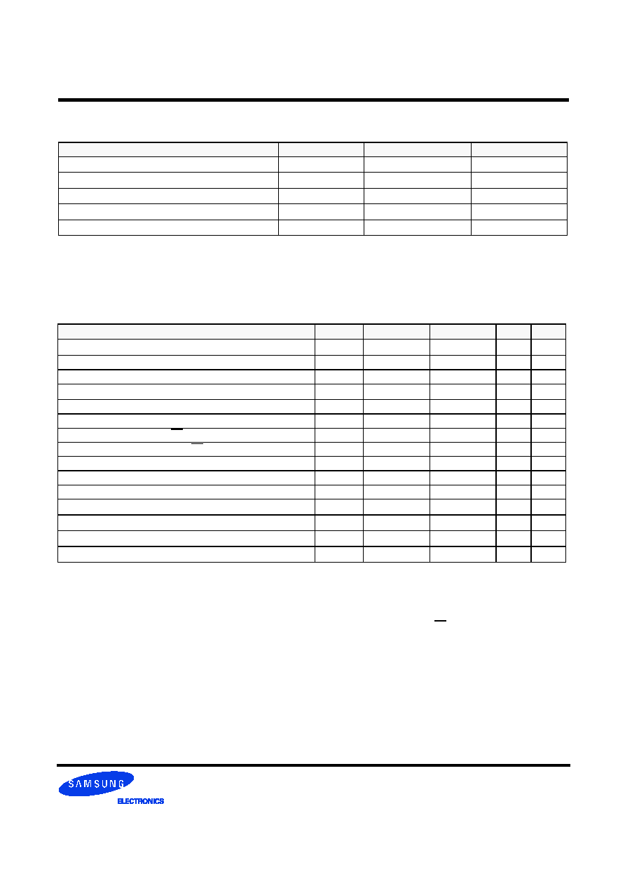
Absolute Maximum Ratings
Parameter
Symbol
Value
Unit
Voltage on any pin relative to VSS
VIN, VOUT
-0.5 ~ 3.6
V
Voltage on VDD & VDDQ supply relative to VSS
VDD, VDDQ
-1.0 ~ 3.6
V
Storage temperature
TSTG
-55 ~ +150
°C
Power dissipation
PD
1.5 * # of component
W
Short circuit current
IOS
50
mA
Note : Permanent device damage may occur if ABSOLUTE MAXIMUM RATINGS are exceeded.
Functional operation should be restricted to recommend operation condition.
Exposure to higher than recommended voltage for extended periods of time could affect device reliability.
DC Operating Conditions
Recommended operating conditions(Voltage referenced to VSS=0V, TA=0 to 70
°C)
Parameter
Symbol
Min
Max
Unit
Note
Supply voltage(for device with a nominal VDD of 2.5V)
VDD
2.3
2.7
I/O Supply voltage
VDDQ
2.3
2.7
V
I/O Reference voltage
VREF
0.49*VDDQ
0.51*VDDQ
V
1
I/O Termination voltage(system)
VTT
VREF-0.04
VREF+0.04
V2
Input logic high voltage
VIH(DC)
VREF+0.15
VDDQ+0.3
V
Input logic low voltage
VIL(DC)
-0.3
VREF-0.15
V
Input Voltage Level, CK and CK inputs
VIN(DC)
-0.3
VDDQ+0.3
V
Input Differential Voltage, CK and CK inputs
VID(DC)
0.36
VDDQ+0.6
V
3
V-I Matching: Pullup to Pulldown Current Ratio
VI(Ratio)
0.71
1.4
-
4
Input leakage current
II
-2
2
uA
Output leakage current
IOZ
-5
5
uA
Output High Current(Normal strengh driver) ;VOUT = VTT + 0.84V
IOH
-16.8
mA
Output High Current(Normal strengh driver) ;VOUT = VTT - 0.84V
IOL
16.8
mA
Output High Current(Half strengh driver) ;VOUT = VTT + 0.45V
IOH
-9
mA
Output High Current(Half strengh driver) ;VOUT = VTT - 0.45V
IOL
9mA
1.VREF is expected to be equal to 0.5*VDDQ of the transmitting device, and to track variations in the dc level of same.
Peak-to peak noise on VREF may not exceed +/-2% of the dc value.
2. VTT is not applied directly to the device. VTT is a system supply for signal termination resistors, is expected to be set equal to
VREF, and must track variations in the DC level of VREF
3. VID is the magnitude of the difference between the input level on CK and the input level on CK.
4. The ratio of the pullup current to the pulldown current is specified for the same temperature and voltage, over the entire
temperature and voltage range, for device drain to source voltages from 0.25V to 1.0V. For a given output, it represents the
maximum difference between pullup and pulldown drivers due to process variation. The full variation in the ratio of the
maximum to minimum pullup and pulldown current will not exceed 1/7 for device drain to source voltages from 0.1 to 1.0.
Note :
相關PDF資料 |
PDF描述 |
|---|---|
| M38220MCMFS | 50000 SYSTEM GATE 2.5 VOLT FPGA - NOT RECOMMENDED for NEW DESIGN |
| M38220E1FP | SINGLE-CHIP 8-BIT CMOS MICROCOMPUTER |
| M38220E1FS | SINGLE-CHIP 8-BIT CMOS MICROCOMPUTER |
| M38220E1GP | SINGLE-CHIP 8-BIT CMOS MICROCOMPUTER |
| M38220MCHXXXFP | SINGLE-CHIP 8-BIT CMOS MICROCOMPUTER |
相關代理商/技術參數(shù) |
參數(shù)描述 |
|---|---|
| M381L2923CUM-CB300 | 制造商:Samsung Semiconductor 功能描述:512MSDDDR_MDDR SDRAM MODULX72TSOP2-400(LF) - Bulk |
| M381L6423ETM-CA200 | 制造商:Samsung Semiconductor 功能描述:256 DDR SDRAM MODUL X72 TSOP2-400 - Trays |
| M3820 | 功能描述:電纜固定件和配件 LTRSCG 875 BLACK RoHS:否 制造商:Heyco 類型:Cable Grips, Liquid Tight 材料:Nylon 顏色:Black 安裝方法:Cable 最大光束直徑:11.4 mm 抗拉強度: |
| M38203 | 制造商:MITSUBISHI 制造商全稱:Mitsubishi Electric Semiconductor 功能描述:8-BIT SINGLE-CHIP MICROCOMPUTER |
| M38203E4 | 制造商:MITSUBISHI 制造商全稱:Mitsubishi Electric Semiconductor 功能描述:SINGLE-CHIP 8-BIT CMOS MICROCOMPUTER |
發(fā)布緊急采購,3分鐘左右您將得到回復。