- 您現(xiàn)在的位置:買賣IC網(wǎng) > PDF目錄69013 > M37549G1-XXXFP 8-BIT, MROM, 8 MHz, MICROCONTROLLER, PDSO24 PDF資料下載
參數(shù)資料
| 型號(hào): | M37549G1-XXXFP |
| 元件分類: | 微控制器/微處理器 |
| 英文描述: | 8-BIT, MROM, 8 MHz, MICROCONTROLLER, PDSO24 |
| 封裝: | 5.30 X 10.10 MM, 0.80 MM PITCH, PLASTIC, SSOP-24 |
| 文件頁數(shù): | 37/86頁 |
| 文件大小: | 1375K |
| 代理商: | M37549G1-XXXFP |
第1頁第2頁第3頁第4頁第5頁第6頁第7頁第8頁第9頁第10頁第11頁第12頁第13頁第14頁第15頁第16頁第17頁第18頁第19頁第20頁第21頁第22頁第23頁第24頁第25頁第26頁第27頁第28頁第29頁第30頁第31頁第32頁第33頁第34頁第35頁第36頁當(dāng)前第37頁第38頁第39頁第40頁第41頁第42頁第43頁第44頁第45頁第46頁第47頁第48頁第49頁第50頁第51頁第52頁第53頁第54頁第55頁第56頁第57頁第58頁第59頁第60頁第61頁第62頁第63頁第64頁第65頁第66頁第67頁第68頁第69頁第70頁第71頁第72頁第73頁第74頁第75頁第76頁第77頁第78頁第79頁第80頁第81頁第82頁第83頁第84頁第85頁第86頁
Rev.2.02
Mar 31, 2009
Page 40 of 81
REJ03B0202-0202
7549 Group
A/D Converter
The functional blocks of the A/D converter are described below.
[AD conversion register] AD
The A/D conversion register is a read-only register that stores the
result of A/D conversion. Do not read out this register during an
A/D conversion.
[AD control register] ADCON
The AD control register controls the A/D converter.
Bit 2 to 0 are analog input pin selection bits.
Bit 3 is the AD conversion clock selection bit. When “0” is set to
this bit, the A/D conversion clock is
φSOURCE/2 and the A/D
conversion time is 122 cycles of
φSOURCE. When “1” is set to
this bit, the A/D conversion clock is
φSOURCE and the A/D
conversion time is 61 cycles of
φSOURCE.
Bit 4 is the AD conversion completion bit. The value of this bit
remains at “0” during A/D conversion, and changes to “1” at
completion of A/D conversion.
A/D conversion is started by setting this bit to “0”.
[Comparison voltage generator]
The comparison voltage generator divides the voltage between
VSS and VCC by 1024, and outputs the divided voltages.
[Channel selector]
The channel selector selects one of ports P17/AN7 to P10/AN0,
and inputs the voltage to the comparator.
[Comparator and control circuit]
The comparator and control circuit compares an analog input
voltage with the comparison voltage and stores its result into the
AD conversion register. When AD conversion is completed, the
control circuit sets the AD conversion completion bit and the A/
D conversion interrupt request bit to “1”. Because the
comparator is constructed linked to a capacitor, set
φSOURCE in
order that the A/D conversion clock is 250 kHz or over during A/
D conversion.
Notes
As for A/D translation accuracy, on the following operating
conditions, accuracy may become low.
(1) When VCC voltage is lower than [3.0 V], the accuracy at the
low temperature may become extremely low compared with
that at room temperature. When the system would be used at
low temperature, the use at VCC = 3.0 V or more is
recommended.
(2) When XCIN or the low-speed on-chip oscillator is selected as
φSOURCE, the A/D converter cannot be used.
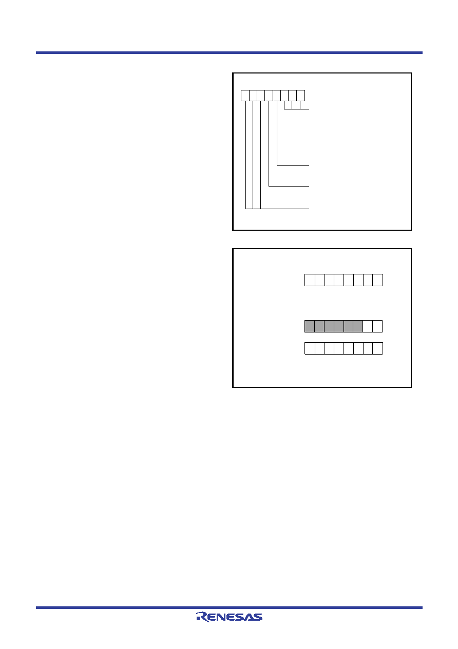
Fig 50. Structure of AD control register
Fig 51. Structure of AD conversion register
AD control register
(ADCON: address 003416, initial value: 1016)
Analog input pin selection bits
000: P10/AN0
001: P11/AN1
010: P12/AN2
011: P13/AN3
100: P14/AN4
101: P15/AN5
110: P16/AN6
111: P17/AN7
AD conversion clock selection bit
0:
φSOURCE/2
1:
φSOURCE
AD conversion completion bit
0: Conversion in progress
1: Conversion completed
Not used (returns “0” when read)
b7
b0
Read 8-bit (Read only address 003516)
(Address 003516)
Read 10-bit (read in order address 003616, 003516)
(Address 003616)
(Address 003516)
Note: High-order 6-bit of address 003616 returns “0” when read.
b7
b0
b9 b8
b7
b0
b6 b5 b4 b3 b2 b1 b0
b9
b7
b0
b8 b7 b6 b5 b4 b3 b2
相關(guān)PDF資料 |
PDF描述 |
|---|---|
| M37549G1FP | 8-BIT, MROM, 8 MHz, MICROCONTROLLER, PDSO24 |
| M37560M8-XXXFP | 8-BIT, MROM, 8 MHz, MICROCONTROLLER, PQFP100 |
| M37560EFDFP | 8-BIT, OTPROM, 8 MHz, MICROCONTROLLER, PQFP100 |
| M37560MFD-XXXFP | 8-BIT, MROM, 8 MHz, MICROCONTROLLER, PQFP100 |
| M37560EFFP | 8-BIT, OTPROM, 8 MHz, MICROCONTROLLER, PQFP100 |
相關(guān)代理商/技術(shù)參數(shù) |
參數(shù)描述 |
|---|---|
| M37549G2FP | 制造商:RENESAS 制造商全稱:Renesas Technology Corp 功能描述:SINGLE-CHIP 8-BIT CMOS MICROCOMPUTER |
| M37549G2-XXXFP | 制造商:RENESAS 制造商全稱:Renesas Technology Corp 功能描述:SINGLE-CHIP 8-BIT CMOS MICROCOMPUTER |
| M37549G3FP | 制造商:RENESAS 制造商全稱:Renesas Technology Corp 功能描述:SINGLE-CHIP 8-BIT CMOS MICROCOMPUTER |
| M37549G3-XXXFP | 制造商:RENESAS 制造商全稱:Renesas Technology Corp 功能描述:SINGLE-CHIP 8-BIT CMOS MICROCOMPUTER |
| M37549RLSS | 制造商:RENESAS 制造商全稱:Renesas Technology Corp 功能描述:SINGLE-CHIP 8-BIT CMOS MICROCOMPUTER |
發(fā)布緊急采購,3分鐘左右您將得到回復(fù)。