- 您現(xiàn)在的位置:買賣IC網(wǎng) > PDF目錄98004 > M306K9FCLRP 16-BIT, FLASH, 16 MHz, MICROCONTROLLER, PQFP144 PDF資料下載
參數(shù)資料
| 型號: | M306K9FCLRP |
| 元件分類: | 微控制器/微處理器 |
| 英文描述: | 16-BIT, FLASH, 16 MHz, MICROCONTROLLER, PQFP144 |
| 封裝: | 16 X 16 MM, 0.40 MM PITCH, PLASTIC, TQFP-144 |
| 文件頁數(shù): | 24/294頁 |
| 文件大?。?/td> | 2600K |
| 代理商: | M306K9FCLRP |
第1頁第2頁第3頁第4頁第5頁第6頁第7頁第8頁第9頁第10頁第11頁第12頁第13頁第14頁第15頁第16頁第17頁第18頁第19頁第20頁第21頁第22頁第23頁當(dāng)前第24頁第25頁第26頁第27頁第28頁第29頁第30頁第31頁第32頁第33頁第34頁第35頁第36頁第37頁第38頁第39頁第40頁第41頁第42頁第43頁第44頁第45頁第46頁第47頁第48頁第49頁第50頁第51頁第52頁第53頁第54頁第55頁第56頁第57頁第58頁第59頁第60頁第61頁第62頁第63頁第64頁第65頁第66頁第67頁第68頁第69頁第70頁第71頁第72頁第73頁第74頁第75頁第76頁第77頁第78頁第79頁第80頁第81頁第82頁第83頁第84頁第85頁第86頁第87頁第88頁第89頁第90頁第91頁第92頁第93頁第94頁第95頁第96頁第97頁第98頁第99頁第100頁第101頁第102頁第103頁第104頁第105頁第106頁第107頁第108頁第109頁第110頁第111頁第112頁第113頁第114頁第115頁第116頁第117頁第118頁第119頁第120頁第121頁第122頁第123頁第124頁第125頁第126頁第127頁第128頁第129頁第130頁第131頁第132頁第133頁第134頁第135頁第136頁第137頁第138頁第139頁第140頁第141頁第142頁第143頁第144頁第145頁第146頁第147頁第148頁第149頁第150頁第151頁第152頁第153頁第154頁第155頁第156頁第157頁第158頁第159頁第160頁第161頁第162頁第163頁第164頁第165頁第166頁第167頁第168頁第169頁第170頁第171頁第172頁第173頁第174頁第175頁第176頁第177頁第178頁第179頁第180頁第181頁第182頁第183頁第184頁第185頁第186頁第187頁第188頁第189頁第190頁第191頁第192頁第193頁第194頁第195頁第196頁第197頁第198頁第199頁第200頁第201頁第202頁第203頁第204頁第205頁第206頁第207頁第208頁第209頁第210頁第211頁第212頁第213頁第214頁第215頁第216頁第217頁第218頁第219頁第220頁第221頁第222頁第223頁第224頁第225頁第226頁第227頁第228頁第229頁第230頁第231頁第232頁第233頁第234頁第235頁第236頁第237頁第238頁第239頁第240頁第241頁第242頁第243頁第244頁第245頁第246頁第247頁第248頁第249頁第250頁第251頁第252頁第253頁第254頁第255頁第256頁第257頁第258頁第259頁第260頁第261頁第262頁第263頁第264頁第265頁第266頁第267頁第268頁第269頁第270頁第271頁第272頁第273頁第274頁第275頁第276頁第277頁第278頁第279頁第280頁第281頁第282頁第283頁第284頁第285頁第286頁第287頁第288頁第289頁第290頁第291頁第292頁第293頁第294頁
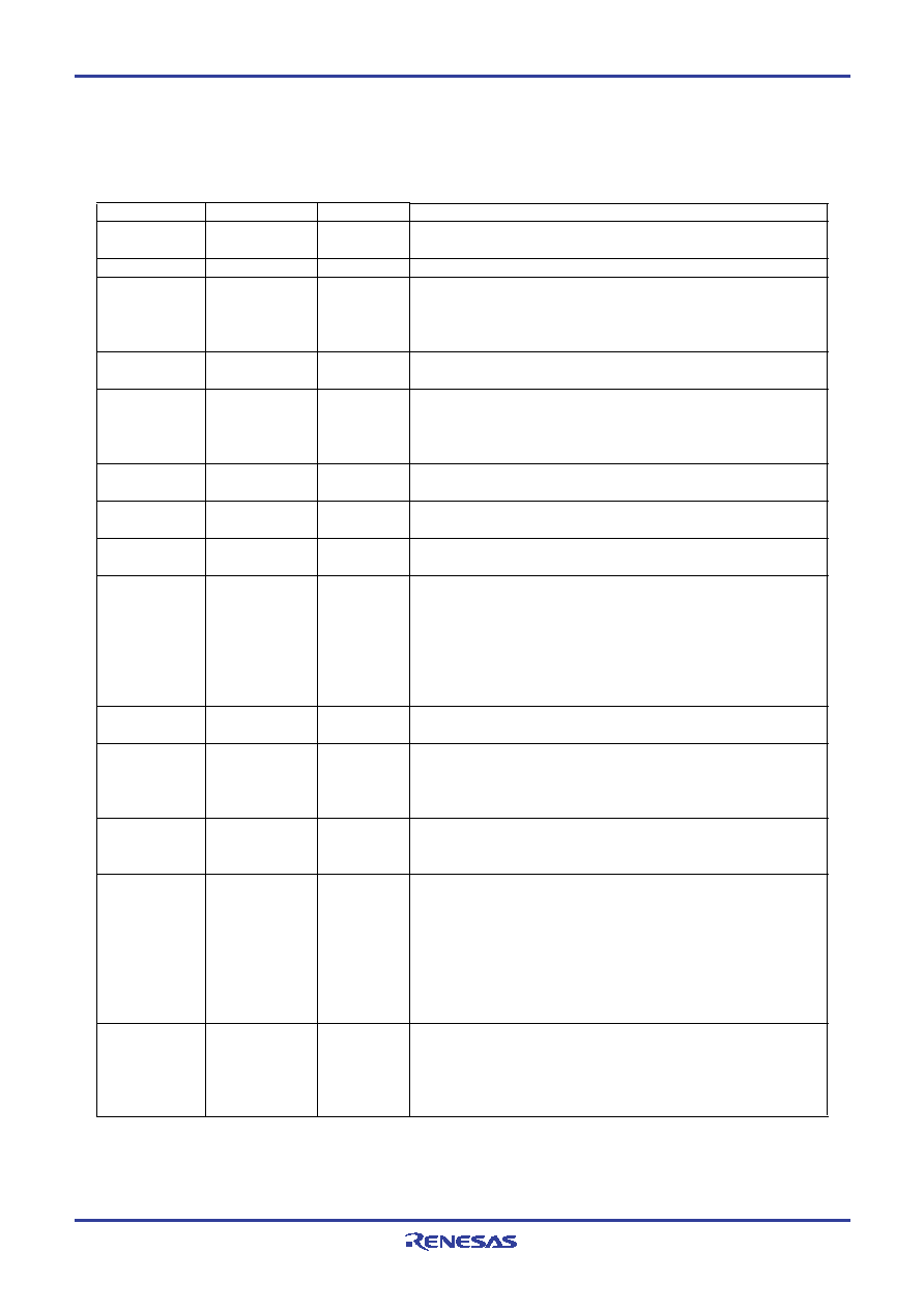
Pin Description
Rev.1.00
Jun 06, 2003
page 10 of 290
M16C/6K9 Group
Pin Description
Signal name
Power supply
input
Reset input
Clock input
Clock output
Chip mode
setting
Power supply
input for flash
memory pro-
gramming
Analog power
supply input
Analog power
supply input
Reference
voltage input
I/O port P0
I/O port P1
I/O port P2
I/O port P3
I/O port P4
I/O port P5
I/O type
Input
Output
Input
Input/output
Function
Apply 3.0 to 3.6 V to VCC . Apply 0V to VSS
A “L” on this input resets the microcomputer.
These pins are provided for the main clock generating circuit.
Connect a ceramic resonator or crystal between the XIN and
the XOUT pins. To use an externally derived clock, input it to
the XIN pin and leave the XOUT pin open.
Connect to VSS
This pin is a power supply input for on-chip flash memory
programming. During the normal operation, 0V to 3.6V can
be applied. When programming on-chip flash memory, 3.0V
to 3.6V should be applied.
This pin is a power supply input for the A-D converter.
Connect this pin to VCC.
This pin is a power supply input for the A-D converter.
Connect this pin to VSS.
This pin is a reference voltage input for the A-D converter.
This is an 8-bit CMOS I/O port. It has an input/output port
direction register that allows the user to set each pin for in-
put or output individually. When set for input, the user can
specify in units of four bits via software whether or not they
are tied to a pull-up resistor.
This port supports CMOS input level. And output type sup-
ports CMOS 3 state or N channel open drain selectable.
This is an 8-bit I/O port equivalent to P0. Pins in this port also
function as external interrupt pins as selected by software.
This is an 8-bit I/O port equivalent to P0. (Except that output
type just supports CMOS 3 state only). P20-P27 are avail-
able for directly driving LED's.P20 to P24 also function as
UART2 or SI/O pins as selected by software.
This is an 8-bit I/O port equivalent to P0. (Except that output
type just supports CMOS 3 state only). The port can be
used for LPC bus interface I/O pins by software selection.
This is an 8-bit I/O port equivalent to P0. (Except that output
type just supports CMOS 3 state only). By software selecting,
the port can also be used for LPC bus interface I/O pins,
Timer A0 to A2 output pins PWM output pins or serial interrupt
output I/O pins. P40 to P46 pins' level can be read regardless
the setting of input port or output port. If P40 or P43 are used
for output ports, the function that clears P40 or P43 to "0" after
the read of output data buffer from host CPU is available.
This is an 8-bit I/O port equivalent to P0. (Except that output type
is CMOS 3 state only). Key on wake interrupt 0 and comparator
input function support. P57 in this port outputs a divide-by-8 or
divide-by-32 clock of XIN or a clock of the same frequency as
XCIN as selected by software.
Pin name
Vcc, Vss
____________
RESET
XIN
XOUT
M0,M1
FVCC
AVCC
AVSS
VREF
P00 to P07
P10 to P17
P20 to P27
P30 to P37
P40 to P47
P50 to P57
相關(guān)PDF資料 |
PDF描述 |
|---|---|
| M306N0MCT-XXXFP | 16-BIT, MROM, 20 MHz, MICROCONTROLLER, PQFP100 |
| M306V2EEFS | 16-BIT, UVPROM, 10 MHz, MICROCONTROLLER, CQCC100 |
| M306V5EESP | 16-BIT, OTPROM, 10 MHz, MICROCONTROLLER, PDIP64 |
| M306V5EESP | 16-BIT, OTPROM, 10 MHz, MICROCONTROLLER, PDIP64 |
| M30800SAGP | 32-BIT, 32 MHz, MICROCONTROLLER, PQFP100 |
相關(guān)代理商/技術(shù)參數(shù) |
參數(shù)描述 |
|---|---|
| M306K9T2-CPE | 功能描述:M-SUPPORT TOOL RoHS:否 類別:編程器,開發(fā)系統(tǒng) >> 內(nèi)電路編程器、仿真器以及調(diào)試器 系列:- 產(chǎn)品變化通告:Development Systems Discontinuation 19/Jul/2010 標(biāo)準(zhǔn)包裝:1 系列:* 類型:* 適用于相關(guān)產(chǎn)品:* 所含物品:* |
| M306KAFCLRP | 制造商:RENESAS 制造商全稱:Renesas Technology Corp 功能描述:SINGLE-CHIP 16-BIT CMOS MICROCOMPUTER Description |
| M306N0FG | 制造商:MITSUBISHI 制造商全稱:Mitsubishi Electric Semiconductor 功能描述:SINGLE-CHIP 16-BIT CMOS MICROCOMPUTER |
| M306N0FGT | 制造商:MITSUBISHI 制造商全稱:Mitsubishi Electric Semiconductor 功能描述:SINGLE-CHIP 16-BIT CMOS MICROCOMPUTER |
| M306N0FGTFP | 制造商:Mitsubishi Electric 功能描述: |
發(fā)布緊急采購,3分鐘左右您將得到回復(fù)。