- 您現(xiàn)在的位置:買賣IC網(wǎng) > PDF目錄39416 > LTC2274IUJ (LINEAR TECHNOLOGY CORP) 1-CH 16-BIT PROPRIETARY METHOD ADC, SERIAL ACCESS, PQCC40 PDF資料下載
參數(shù)資料
| 型號: | LTC2274IUJ |
| 廠商: | LINEAR TECHNOLOGY CORP |
| 元件分類: | ADC |
| 英文描述: | 1-CH 16-BIT PROPRIETARY METHOD ADC, SERIAL ACCESS, PQCC40 |
| 封裝: | 6 X 6 MM, PLASTIC, QFN-40 |
| 文件頁數(shù): | 10/40頁 |
| 文件大小: | 897K |
| 代理商: | LTC2274IUJ |
第1頁第2頁第3頁第4頁第5頁第6頁第7頁第8頁第9頁當前第10頁第11頁第12頁第13頁第14頁第15頁第16頁第17頁第18頁第19頁第20頁第21頁第22頁第23頁第24頁第25頁第26頁第27頁第28頁第29頁第30頁第31頁第32頁第33頁第34頁第35頁第36頁第37頁第38頁第39頁第40頁
LTC2274
18
2274fb
APPLICATIONS INFORMATION
SAMPLE/HOLD OPERATION AND INPUT DRIVE
Sample/Hold Operation
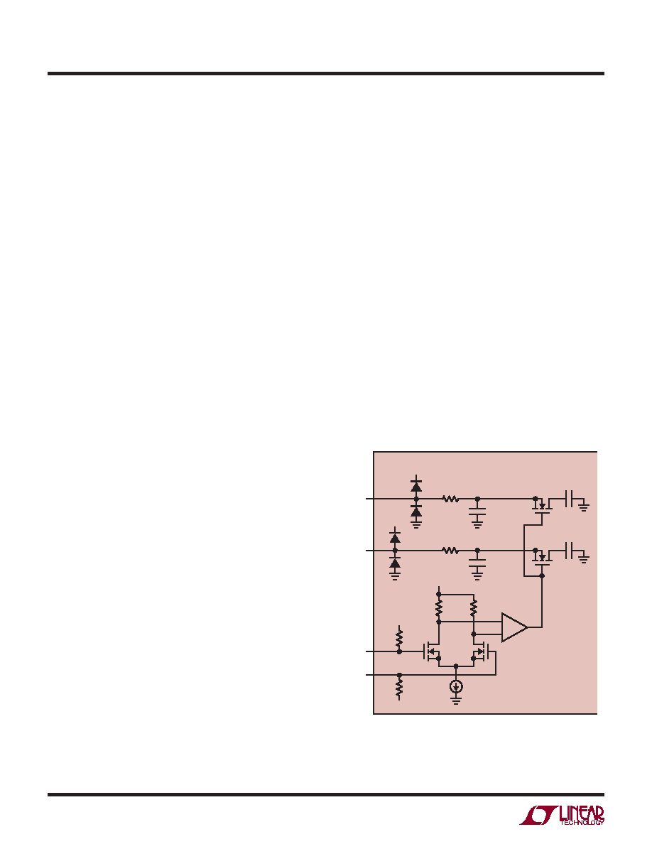
Figure 2 shows an equivalent circuit for the LTC2274 CMOS
differential sample and hold. The differential analog inputs
are sampled directly onto sampling capacitors (CSAMPLE)
through NMOS transistors. The capacitors shown attached
to each input (CPARASITIC) are the summation of all other
capacitance associated with each input.
During the sample phase when ENC is low, the NMOS
transistors connect the analog inputs to the sampling
capacitors and they charge to, and track, the differential
input voltage. On the rising edge of ENC, the sampled
input voltage is held on the sampling capacitors. During
the hold phase when ENC is high, the sampling capacitors
are disconnected from the input and the held voltage is
passed to the ADC core for processing. As ENC transitions
for high to low, the inputs are reconnected to the sampling
capacitors to acquire a new sample. Since the sampling
capacitors still hold the previous sample, a charging glitch
proportional to the change in voltage between samples will
be seen at this time. If the change between the last sample
and the new sample is small, the charging glitch seen at
the input will be small. If the input change is large, such
as the change seen with input frequencies near Nyquist,
then a larger charging glitch will be seen.
Common Mode Bias
The ADC sample-and-hold circuit requires differential drive
to achieve specied performance. Each input should swing
±0.5625V for the 2.25V range (PGA = 0) or ±0.375V for
the 1.5V range (PGA = 1), around a common mode volt-
age of 1.25V. The VCM output pin (Pin 39) is designed to
provide the common mode bias level. VCM can be tied
directly to the center tap of a transformer to set the DC
input level or as a reference level to an op amp differential
driver circuit. The VCM pin must be bypassed to ground
close to the ADC with 2.2μF or greater.
Input Drive Impedance
As with all high performance, high speed ADCs the dy-
namic performance of the LTC2274 can be inuenced
by the input drive circuitry, particularly the second and
third harmonics. Source impedance and input reactance
can inuence SFDR. At the falling edge of ENC the
sample-and-hold circuit will connect the 4.9pF sampling
capacitor to the input pin and start the sampling period.
The sampling period ends when ENC rises, holding the
sampled input on the sampling capacitor. Ideally, the
input circuitry should be fast enough to fully charge
the sampling capacitor during the sampling period
1/(2FENCODE); however, this is not always possible and the
incomplete settling may degrade the SFDR. The sampling
glitch has been designed to be as linear as possible to
minimize the effects of incomplete settling.
For the best performance it is recommended to have a
source impedance of 100
Ω or less for each input. The
source impedance should be matched for the differential
inputs. Poor matching will result in higher even order
harmonics, especially the second.
CSAMPLE
4.9pF
VDD
LTC2274
AIN+
2274 F02
CSAMPLE
4.9pF
VDD
AIN–
ENC–
ENC+
1.6V
6k
1.6V
6k
CPARASITIC
1.8pF
CPARASITIC
1.8pF
RPARASITIC
3Ω
RON
20Ω
RON
20Ω
RPARASITIC
3Ω
Figure 2. Equivalent Input Circuit
相關(guān)PDF資料 |
PDF描述 |
|---|---|
| LTC2285IUP#3CGPBF | PROPRIETARY METHOD ADC, PQCC64 |
| LTC2305CDE#PBF | 2-CH 12-BIT SUCCESSIVE APPROXIMATION ADC, SERIAL ACCESS, PDSO12 |
| LTC2305CMS#PBF | 2-CH 12-BIT SUCCESSIVE APPROXIMATION ADC, SERIAL ACCESS, PDSO12 |
| LTC2305IDE#PBF | 2-CH 12-BIT SUCCESSIVE APPROXIMATION ADC, SERIAL ACCESS, PDSO12 |
| LTC2305IDE#TRPBF | 2-CH 12-BIT SUCCESSIVE APPROXIMATION ADC, SERIAL ACCESS, PDSO12 |
相關(guān)代理商/技術(shù)參數(shù) |
參數(shù)描述 |
|---|---|
| LTC2274IUJ#PBF | 制造商:Linear Technology 功能描述:ADC Single Pipelined 105Msps 16-bit Serial 40-Pin QFN EP 制造商:Linear Technology 功能描述:IC ADC 16-BIT 105MSPS 40-QFN 制造商:Linear Technology 功能描述:IC ADC 16BIT 105MSPS QFN-40 制造商:Linear Technology 功能描述:IC, ADC, 16BIT, 105MSPS, QFN-40; Resolution (Bits):16bit; Sampling Rate:105MSPS; Supply Voltage Type:Single; Supply Voltage Min:3.135V; Supply Voltage Max:3.465V; Supply Current:394mA; Digital IC Case Style:QFN; No. of Pins:40 ;RoHS Compliant: Yes |
| LTC2274IUJ#TRPBF | 制造商:Linear Technology 功能描述:ADC Single Pipelined 105Msps 16-bit Serial 40-Pin QFN EP T/R 制造商:Linear Technology 功能描述:IC ADC 16-BIT 105MSPS 40-QFN |
| LTC2274IUJ-PBF | 制造商:LINER 制造商全稱:Linear Technology 功能描述:16-Bit, 105Msps Serial Output ADC |
| LTC2274IUJ-TR | 制造商:LINER 制造商全稱:Linear Technology 功能描述:16-Bit, 105Msps Serial Output ADC |
| LTC2274IUJ-TRPBF | 制造商:LINER 制造商全稱:Linear Technology 功能描述:16-Bit, 105Msps Serial Output ADC |
發(fā)布緊急采購,3分鐘左右您將得到回復(fù)。