- 您現(xiàn)在的位置:買賣IC網(wǎng) > PDF目錄377730 > LTC1090M (Linear Technology Corporation) Single Chip 10-Bit Data Acquisition System PDF資料下載
參數(shù)資料
| 型號(hào): | LTC1090M |
| 廠商: | Linear Technology Corporation |
| 英文描述: | Single Chip 10-Bit Data Acquisition System |
| 中文描述: | 單芯片10位數(shù)據(jù)采集系統(tǒng) |
| 文件頁數(shù): | 12/28頁 |
| 文件大小: | 344K |
| 代理商: | LTC1090M |
第1頁第2頁第3頁第4頁第5頁第6頁第7頁第8頁第9頁第10頁第11頁當(dāng)前第12頁第13頁第14頁第15頁第16頁第17頁第18頁第19頁第20頁第21頁第22頁第23頁第24頁第25頁第26頁第27頁第28頁
12
LTC1090
1090fc
Unipolar Output Code (UNI = 1)
INPUT VOLTAGE
(V
REF
= 5V)
4.9951V
4.9902V
0.0049V
0V
OUTPUT CODE
1111111111
1111111110
0000000001
0000000000
INPUT VOLTAGE
V
REF
– 1LSB
V
REF
– 2LSB
1LSB
0V
Bipolar Output Code (UNI = 0)
INPUT VOLTAGE
(V
REF
= 5V)
4.9902V
4.9805V
0.0098V
0V
–0.0098V
–0.0195V
–4.9902V
–5.000V
OUTPUT CODE
0111111111
0111111110
0000000001
0000000000
1111111111
1111111110
1000000001
1000000000
INPUT VOLTAGE
V
REF
– 1LSB
V
REF
– 2LSB
1LSB
0V
–2LSB
– (V
REF
) + 1LSB
– (V
REF
)
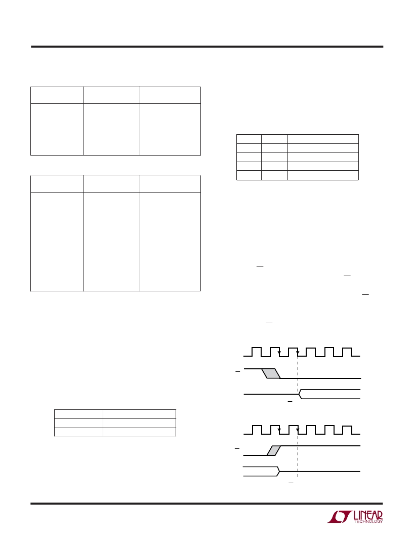
MSB First/LSB First Format (MSBF)
The output data of the LTC1090 is programmed for MSB
first or LSB first sequence using the MSBF bit. For MSB
first output data the input word clocked to the LTC1090
should always contain a logical one in the sixth bit location
(MSBF bit). Likewise for LSB first output data, the input
word clocked to the LTC1090 should always contain a zero
in the MSBF bit location. The MSBF bit in a given D
IN
word
will control the order of the next D
OUT
word. The MSBF bit
affects only the order of the output data word. The order
of the input word is unaffected by this bit.
MSBF
0
1
OUTPUT FORMAT
LSB First
MSB First
Word Length (WL1, WL0)
The last two bits of the input word (WL1 and WL0) program
the output data word length of the LTC1090. Word lengths
of 8, 10, 12 or 16 bits can be selected according to the
following table. The WL1 and WL0 bits in a given D
IN
word
control the length of the present, not the next, D
OUT
word.
WL1 and WL0 are never “don’t cares”
and must be set for
the correct D
OUT
word length even when a “dummy” D
IN
word is sent. On any transfer cycle, the word length should
be made equal to the number of SCLK cycles sent by the
MPU.
WL1
0
0
1
1
WL0
0
1
0
1
OUTPUT WORD LENGTH
8 Bits
10 Bits
12 Bits
16 Bits
Figure 2 shows how the data output (D
OUT
) timing can be
controlled with word length selection and MSB/LSB first
format selection.
3. Deglitcher
A deglitching circuit has been added to the Chip Select
input of the LTC1090 to minimize the effects of errors
caused by noise on that input. This circuit ignores changes
in state on the CS input that are shorter in duration than 1
ACLK cycle. After a change of state on the CS input, the
LTC1090 waits for two falling edges of the ACLK before
recognizing a valid chip select. One indication of CS low
recognition is the D
OUT
line becoming active (leaving the
Hi-Z state). Note that the deglitching applies to both the
rising and falling CS edges.
APPLICATIOU
W
U
U
HIGH Z
HIGH Z
ACLK
ACLK
VALID OUTPUT
D
OUT
D
OUT
CS
CS
LOW CS RECOGNIZED
INTERNALLY
HIGH CS RECOGNIZED
INTERNALLY
LTC1090 AI07
相關(guān)PDF資料 |
PDF描述 |
|---|---|
| LTC1090MJ | Single Chip 10-Bit Data Acquisition System |
| LTC1091AC | 1-, 2-, 6- and 8-Channel, 10-Bit Serial I/O Data Acquisition Systems |
| LTC1091ACN8 | 1-, 2-, 6- and 8-Channel, 10-Bit Serial I/O Data Acquisition Systems |
| LTC1091CN8 | 1-, 2-, 6- and 8-Channel, 10-Bit Serial I/O Data Acquisition Systems |
| LTC1093ACN | 1-, 2-, 6- and 8-Channel, 10-Bit Serial I/O Data Acquisition Systems |
相關(guān)代理商/技術(shù)參數(shù) |
參數(shù)描述 |
|---|---|
| LTC1090MJ | 制造商:LINER 制造商全稱:Linear Technology 功能描述:Single Chip 10-Bit Data Acquisition System |
| LTC1090MJ/883 | 制造商:未知廠家 制造商全稱:未知廠家 功能描述:Single-Ended Data Acquisition System |
| LTC1091 | 制造商:LINER 制造商全稱:Linear Technology 功能描述:1-, 2-, 6- and 8-Channel, 10-Bit Serial I/O Data Acquisition Systems |
| LTC1091AC | 制造商:LINER 制造商全稱:Linear Technology 功能描述:1-, 2-, 6- and 8-Channel, 10-Bit Serial I/O Data Acquisition Systems |
| LTC1091ACJ8 | 制造商:未知廠家 制造商全稱:未知廠家 功能描述:Single-Ended Data Acquisition System |
發(fā)布緊急采購,3分鐘左右您將得到回復(fù)。