- 您現(xiàn)在的位置:買賣IC網(wǎng) > PDF目錄39399 > LT6350IMS8#TRPBF (LINEAR TECHNOLOGY CORP) 1-CH 16-BIT SUCCESSIVE APPROXIMATION ADC, PARALLEL ACCESS, PDSO8 PDF資料下載
參數(shù)資料
| 型號: | LT6350IMS8#TRPBF |
| 廠商: | LINEAR TECHNOLOGY CORP |
| 元件分類: | ADC |
| 英文描述: | 1-CH 16-BIT SUCCESSIVE APPROXIMATION ADC, PARALLEL ACCESS, PDSO8 |
| 封裝: | LEAD FREE, PLASTIC, MSOP-8 |
| 文件頁數(shù): | 11/28頁 |
| 文件大小: | 462K |
| 代理商: | LT6350IMS8#TRPBF |
第1頁第2頁第3頁第4頁第5頁第6頁第7頁第8頁第9頁第10頁當(dāng)前第11頁第12頁第13頁第14頁第15頁第16頁第17頁第18頁第19頁第20頁第21頁第22頁第23頁第24頁第25頁第26頁第27頁第28頁
LT6350
19
6350fb
APPLICATIONS INFORMATION
Because the input bias current into op amp 2 is much larger
than the offset current, choosing R+IN2 to be RINT/2 greatly
reduces the offset contribution of op amp 2’s input currents
on all units. With R+IN2 = RINT/2, VOSCM reduces to:
VOSCM = VOS2 – (IOS2/2) RINT
VOSCM is trimmed to within ±125μV with a 499Ω resistor
installed at +IN2.
The value of VOS1 is trimmed to bring VOSDIFF to ± 125μV.
Because linear modulation of VOS1 with input common
mode could degrade the common mode rejection ratio
specication of op amp 1, and nonlinear modulation of
VOS1 could cause nonlinear gain error (distortion), VOS1
is trimmed to a low constant value over as wide an input
common mode range as possible. A precision, 2-point
trim algorithm is used that results in VOS1 within ±125μV
over the input range V– + 1.3V ≤ V+IN1 ≤ V+ and VOS1
within ±300μV over the input range V– ≤ V+IN1 ≤ V+. A
negative supply below –1.3V can be used to extend the
input range for which VOS1 is within ±125μV all the way
down to ground.
As a result of the trim procedure, the lowest offsets, both
common mode and differential mode, will occur with a
499Ω resistor at +IN2. This resistor can be bypassed with
a capacitor to eliminate its noise contribution. The gain-
setting resistor network (RG and RF) impedance should
be matched to that of the source to minimize op amp 1’s
input bias current contributions to the offsets.
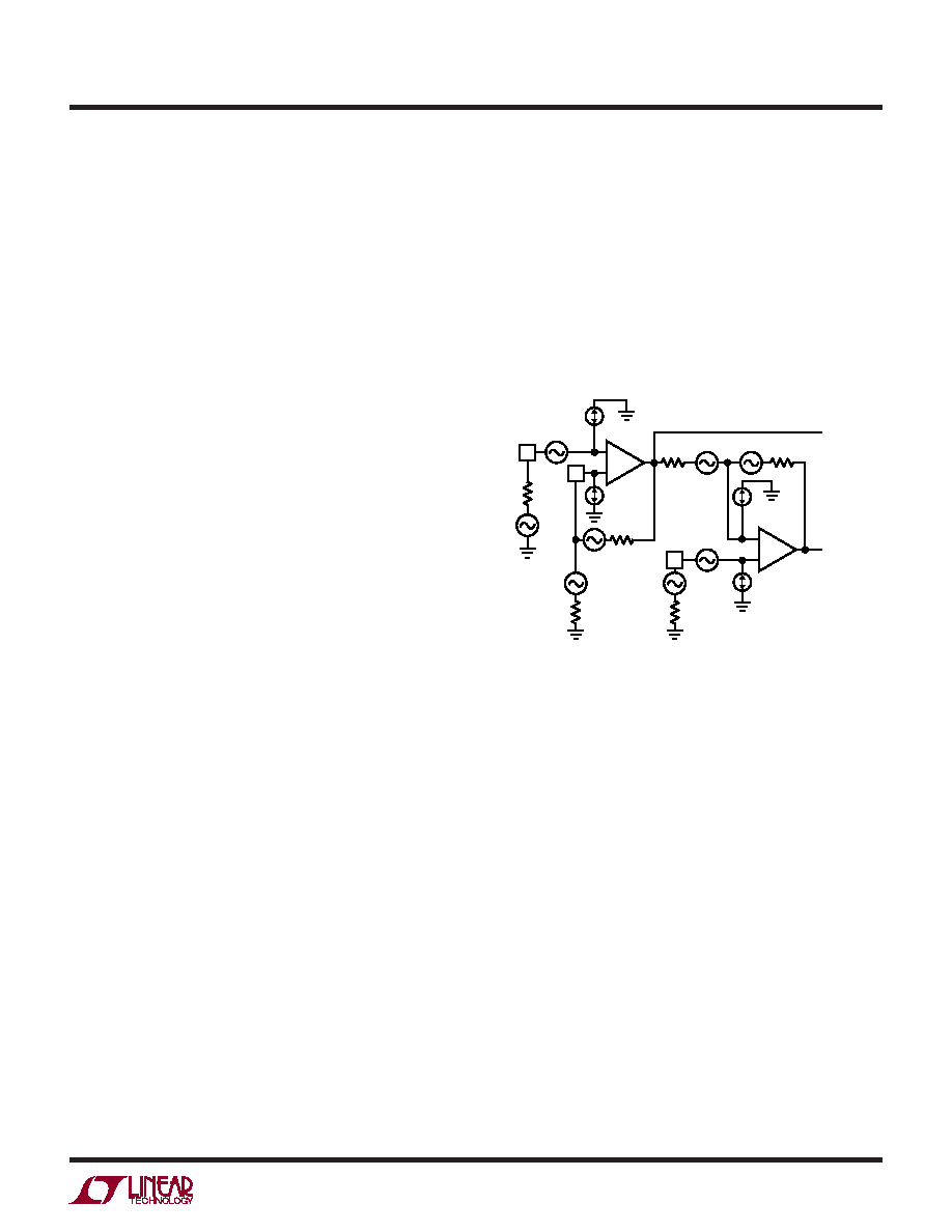
NOISE CONSIDERATIONS
A model showing the sources of output noise in the LT6350
is shown in Figure 8. The total output noise resulting from
all contributors is governed by the equation:
The LT6350 uses very low noise op amps, resulting in a
total differential output spot noise at 10kHz of 8.2nV/√Hz
when the LT6350 is in the noninverting gain-of-two con-
guration shown in Figure 2. This is equivalent to the
voltage noise of a 1015Ω resistor at the +IN1 input. For
source resistors larger than about 1k, voltage noise due to
the source resistance will start to dominate output noise.
Source resistors larger than about 13k will interact with
the input current noise and result in output noise that is
resistor noise and amplier current noise dominant.
–
+
–
RG
RS
R+IN2
RF
RINT
in1
en1
enRF
enRG
enRS
eno1
eno2
–IN1
+IN1
+IN2
OP AMP 1
OP AMP 2
6350 F08
enRINT
en2
enR+IN2
in2
+
eno
–
Figure 8. Noise Model
Note that the parallel combination of gain-setting resis-
tors RF and RG behaves like the source resistance, RS,
from the point of view of noise calculations, and the value
should be kept below about 1k to avoid increasing the
output noise. Lower-value gain and feedback resistors,
eno = √(4 [e2n1 + (in1RS)2 + e2nRS](1 + (RF /RG))2 + 4 (in1RF)2 + 4e2nRF (1 + (RF /RG)) + 4e2n2 + 4e2nR+IN2 +
2e2nRINT + (in2RINT)2 + 4 (in2R+IN2)2 )
相關(guān)PDF資料 |
PDF描述 |
|---|---|
| LT6350IDD#TRPBF | 1-CH 16-BIT SUCCESSIVE APPROXIMATION ADC, PARALLEL ACCESS, PDSO8 |
| LT6350CMS8#PBF | 1-CH 16-BIT SUCCESSIVE APPROXIMATION ADC, PARALLEL ACCESS, PDSO8 |
| LT6350IMS8#PBF | 1-CH 16-BIT SUCCESSIVE APPROXIMATION ADC, PARALLEL ACCESS, PDSO8 |
| LT6350CMS8#TRPBF | 1-CH 16-BIT SUCCESSIVE APPROXIMATION ADC, PARALLEL ACCESS, PDSO8 |
| LT6350HDD#PBF | 1-CH 16-BIT SUCCESSIVE APPROXIMATION ADC, PARALLEL ACCESS, PDSO8 |
相關(guān)代理商/技術(shù)參數(shù) |
參數(shù)描述 |
|---|---|
| LT6360 | 制造商:LINER 制造商全稱:Linear Technology 功能描述:18-Bit, 1.6Msps, Pseudo-Differential Unipolar SAR |
| LT63H-SERIES | 制造商:未知廠家 制造商全稱:未知廠家 功能描述:Optoelectronic |
| LT63HXX-SERIES | 制造商:未知廠家 制造商全稱:未知廠家 功能描述:Optoelectronic |
| LT6402-12 | 制造商:LINER 制造商全稱:Linear Technology 功能描述:1.3GHz Low Noise, Low Distortion Differential ADC Driver for 140MHz IF |
| LT6402-20 | 制造商:LINER 制造商全稱:Linear Technology 功能描述:1.3GHz Low Noise, Low Distortion Differential ADC Driver for 140MHz IF |
發(fā)布緊急采購,3分鐘左右您將得到回復(fù)。