- 您現(xiàn)在的位置:買賣IC網(wǎng) > PDF目錄361044 > LMX9820A (National Semiconductor Corporation) Bluetooth Serial Port Module PDF資料下載
參數(shù)資料
| 型號: | LMX9820A |
| 廠商: | National Semiconductor Corporation |
| 英文描述: | Bluetooth Serial Port Module |
| 中文描述: | 藍牙串行端口模塊 |
| 文件頁數(shù): | 10/44頁 |
| 文件大?。?/td> | 579K |
| 代理商: | LMX9820A |
第1頁第2頁第3頁第4頁第5頁第6頁第7頁第8頁第9頁當(dāng)前第10頁第11頁第12頁第13頁第14頁第15頁第16頁第17頁第18頁第19頁第20頁第21頁第22頁第23頁第24頁第25頁第26頁第27頁第28頁第29頁第30頁第31頁第32頁第33頁第34頁第35頁第36頁第37頁第38頁第39頁第40頁第41頁第42頁第43頁第44頁
www.national.com
10
Revision 1.0
L
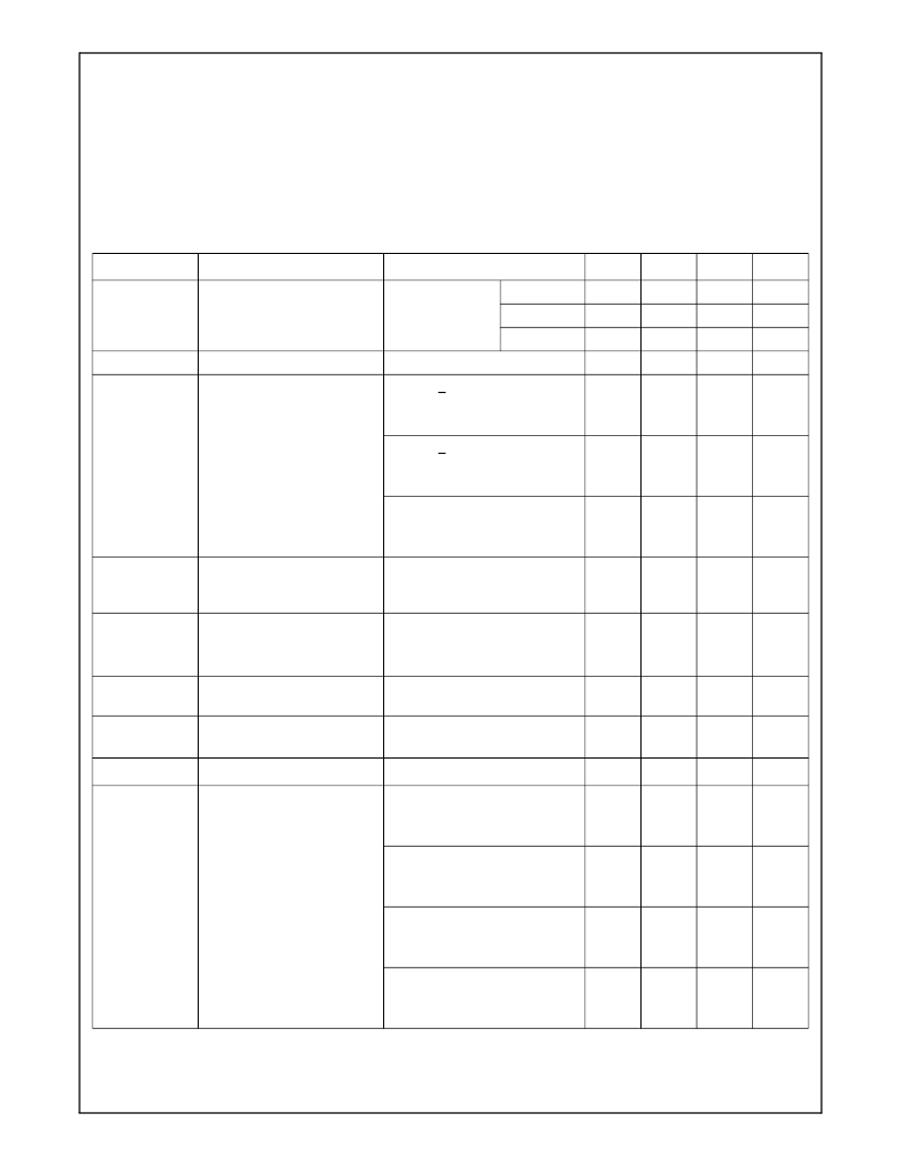
6.0 Electrical Specifications
(Continued)
6.3 RF PERFORMANCE CHARACTERISTICS
In the performance characteristics tables the following
applies:
All tests performed are based on Bluetooth Test Specifi-
cation rev 0.92.
All tests are measured at antenna port unless otherwise
specified
T
A
= -40°C to +85°C
VCC = 3.3V, IOVCC = 3.3V unless otherwise specified
RF system performance specifications are guaranteed on
National Semiconductor Austin Board rev1.0b reference
design platform.
Table 14. Receiver Performance Characteristics
Symbol
Parameter
Condition
Min
Typ
1
Max
Unit
RX
sense
2
Receive Sensitivity
BER < 0.001
2.402 GHz
-81
-77
dBm
2.441 GHz
-81
-77
dBm
2.480 GHz
-81
-77
dBm
PinRF
Maximum Input Level
-10
0
dBm
C/I
ACI3
Carrier to Interferer Ratio in
the Presence of Adjacent
Channel Interferer
F
ACI
= + 1 MHz,
P
in
RF = -60 dBm,
BER < 0.001
-1
dB
F
ACI
= + 2 MHz.
P
in
RF = -60 dBm,
BER < 0.001
-37
dB
F
ACI
= + 3 MHz,
P
in
RF = -67 dBm,
BER < 0.001
-47
dB
C/I
IMAGE
-1MHz
Carrier to Interferer Ratio in
the Presence of Image-1MHz
Interferer
f = -3 MHz,
PinRF = -67 dBm,
BER < 0.001
-32
dB
IMP
3,4
Intermodulation Performance
F
1
= + 3 MHz,
F
2
= + 6 MHz,
P
in
RF = -64 dBm
-38
-36
dBm
RSSI
RSSI Dynamic Range at LNA
Input
-72
-52
dBm
Z
RFIN
Input Impedance of RF Port
(RF_inout)
Single input impedance
F
in
= 2.45 GHz
50
Return Loss
3
Return Loss
-8
dB
OOB
3
Out Of Band Blocking
Performance
P
in
RF = -10 dBm,
30 MHz < F
CWI
< 2 GHz,
BER < 0.001
-10
dBm
P
in
RF = -27 dBm,
2000 MHz < F
CWI
< 2399 MHz,
BER < 0.001
-27
dBm
P
in
RF = -27 dBm,
2498 MHz < F
CWI
< 3000 MHz,
BER < 0.001
-27
dBm
P
in
RF = -10 dBm,
3000 MHz < F
CWI
< 12.75 GHz,
BER < 0.001
-10
dBm
1.
2.
3.
Typical operating conditions are at 2.85V operating voltage and 25°C ambient temperature.
The receiver sensitivity is measured at the device interface.
Not tested in production.
相關(guān)PDF資料 |
PDF描述 |
|---|---|
| LMX9820ASM | Bluetooth Serial Port Module |
| LMX9820 | Bluetooth Serial Port Module |
| LMX9820SB | Bluetooth Serial Port Module |
| LMX9820SBX | Bluetooth Serial Port Module |
| LP3882ESX-1.2 | 1.5A Fast-Response Ultra Low Dropout Linear |
相關(guān)代理商/技術(shù)參數(shù) |
參數(shù)描述 |
|---|---|
| LMX9820ADEV | 制造商:Texas Instruments 功能描述:KIT DEV FOR LMX9820 |
| LMX9820ADONGLE/NOPB | 制造商:Texas Instruments 功能描述:KIT REF DESIGN FOR LMX9820 |
| LMX9820ASM | 制造商:Texas Instruments 功能描述:BLUETOOTH MODULE, SMD, 9820, FR4129 |
| LMX9820ASM/NOPB | 制造商:Texas Instruments 功能描述:IC MODULE BLUETOOTH 116-LTCC |
| LMX9820ASMX | 制造商:NSC 制造商全稱:National Semiconductor 功能描述:Bluetooth Serial Port Module |
發(fā)布緊急采購,3分鐘左右您將得到回復(fù)。