- 您現(xiàn)在的位置:買賣IC網(wǎng) > PDF目錄369797 > LM9820 PDF資料下載
參數(shù)資料
| 型號: | LM9820 |
| 文件頁數(shù): | 5/20頁 |
| 文件大?。?/td> | 245K |
| 代理商: | LM9820 |

LM9820 Electrical Characteristics
(Continued)
The following specifications apply for AGND = DGND = 0V, V
= V
= +5.0V
, f
= 24 MHz, R
= 25
.
Boldface limits
apply for T
= T
J
= T
MIN
to T
MAX
; all other limits T
A
= T
J
= 25C. All LSB limits are in units of the LM9810’s 12-bit ADC.
(Notes 7, 8, 12)
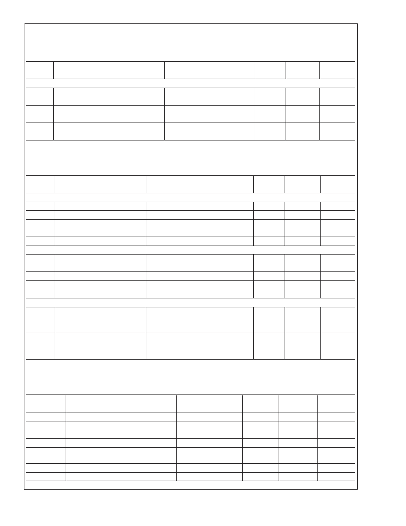
Symbol
Parameter
Conditions
Typical
(Note 9)
Limits
(Note 10)
Units
(Limits)
SYSTEM CHARACTERISTICS (SEE SECTION 1.7.1, INTERNAL OFFSETS)
V
OS1
Pre-Boost Analog Channel Offset Error,
CIS Mode
V
OS2
Pre-PGA Analog Channel Offset Error
18
-22.2
+57
-94.3
+16.4
-121
+28
LSB (min)
LSB (max)
LSB (min)
LSB (max)
LSB (min)
LSB (max)
-40
V
OS3
Post-PGA Analog Channel Offset Error
-44
DC and Logic Electrical Characteristics
The following specifications apply for AGND = DGND = 0V, V
= V
= +5.0V
DC
, f
MCLK
= 24 MHz, R
s
= 25
.
Boldface limits
apply for T
A
= T
J
= T
MIN
to T
MAX
; all other limits T
A
= T
J
= 25C. (Notes 7, 8)
Symbol
Parameter
Conditions
Typical
(Note 9)
Limits
(Note 10)
Units
(Limits)
D0–D2, MCLK, NewLine, SampCLK DIGITAL INPUT CHARACTERISTICS
V
IN(1)
Logical “1” Input Voltage
V
IN(0)
Logical “0” Input Voltage
I
IN
Input Leakage Current
V
D
= 5.25V
V
D
= 4.75V
V
IN
= V
D
V
IN
= DGND
2.0
0.8
V (max)
V (min)
μA (max)
μA (max)
pF
0.1
0.1
5
C
IN
D0–D5, DIGITAL OUTPUT CHARACTERISTICS
V
OUT(1)
Logical “1” Output Voltage
Input Capacitance
V
D
= 4.75V, I
OUT
= 360 μA
V
D
= 4.75V, I
OUT
= 10 μA
V
D
= 5.25V, I
OUT
= 1.6 mA
V
OUT
= DGND
V
OUT
= V
D
2.4
4.4
0.4
V (min)
V (min)
V (max)
μA
μA
V
OUT(0)
I
OUT
Logical “0” Output Voltage
TRI-STATE
Output Current
(D0–D5 only)
POWER SUPPLY CHARACTERISTICS
I
A
Analog Supply Current
0.1
0.1
Operating
Standby with Input Clocks Stopped
Standby with Input Clocks Running
Operating
Standby with Input Clocks Stopped
Standby with Input Clocks Running
45
0.8
3.0
220
110
220
57
0.9
mA (max)
mA (max)
mA
μA (max)
μA (max)
μA
I
D
Digital Supply Current (Note 15)
320
200
AC Electrical Characteristics
The following specifications apply for AGND = DGND = 0V, V
A
= V
D
= +5.0V
, f
= 24 MHz, t
MCLK
= 1/f
MCLK
,
t
r
= t
f
= 5 ns, R
s
= 25
.
Boldface limits apply for T
A
= T
J
= T
MIN
to T
MAX
; all other limits T
A
= T
J
Symbol
Parameter
Conditions
Typical
(Note 9)
Limits
(Note 10)
24
40
60
Units
(Limits)
MHz (min)
f
MCLK
Maximum MCLK Frequency
MCLK Duty Cycle
(min)
(max)
t
MCLK
t
SCNL
MCLK Period
SampCLK Falling Edge before NewLine
Falling Edge
SampCLK Period
Low Time for SampCLK
41
ns (min)
t
MCLK
(min)
3
t
SampCLK
t
SampLo
4
t
MCLK
(min)
ns (min)
50
L
www.national.com
5
相關PDF資料 |
PDF描述 |
|---|---|
| LM9822CCWM | Signal Conditioner |
| LM9822CCWMX | Signal Conditioner |
| LM9823 | |
| LMA110 | .5-6 GHz MESFET Amplifier |
| LMA110A | .5-6 GHz MESFET Amplifier |
相關代理商/技術參數(shù) |
參數(shù)描述 |
|---|---|
| LM9820CCWM | 制造商:NSC 制造商全稱:National Semiconductor 功能描述:LM9810/20 10/12-Bit Image Sensor Processor Analog Front End |
| LM9820CCWMX | 制造商:NSC 制造商全稱:National Semiconductor 功能描述:LM9810/20 10/12-Bit Image Sensor Processor Analog Front End |
| LM9822 | 制造商:NSC 制造商全稱:National Semiconductor 功能描述:LM9822 3 Channel 42-Bit Color Scanner Analog Front End |
| LM9822CCWM | 制造商:Rochester Electronics LLC 功能描述: 制造商:Texas Instruments 功能描述: |
| LM9822CCWM/NOPB | 功能描述:ADC / DAC多通道 RoHS:否 制造商:Texas Instruments 轉(zhuǎn)換速率: 分辨率:8 bit 接口類型:SPI 電壓參考: 電源電壓-最大:3.6 V 電源電壓-最小:2 V 最大工作溫度:+ 85 C 安裝風格:SMD/SMT 封裝 / 箱體:VQFN-40 |
發(fā)布緊急采購,3分鐘左右您將得到回復。