- 您現(xiàn)在的位置:買賣IC網(wǎng) > PDF目錄361035 > LM9811CCV (NATIONAL SEMICONDUCTOR CORP) 10-Bit Greyscale/30-Bit Color Linear CCD Sensor Processor PDF資料下載
參數(shù)資料
| 型號: | LM9811CCV |
| 廠商: | NATIONAL SEMICONDUCTOR CORP |
| 元件分類: | 模擬信號調(diào)理 |
| 英文描述: | 10-Bit Greyscale/30-Bit Color Linear CCD Sensor Processor |
| 中文描述: | SPECIALTY ANALOG CIRCUIT, PQCC52 |
| 封裝: | PLASTIC, LCC-52 |
| 文件頁數(shù): | 21/36頁 |
| 文件大?。?/td> | 605K |
| 代理商: | LM9811CCV |
第1頁第2頁第3頁第4頁第5頁第6頁第7頁第8頁第9頁第10頁第11頁第12頁第13頁第14頁第15頁第16頁第17頁第18頁第19頁第20頁當前第21頁第22頁第23頁第24頁第25頁第26頁第27頁第28頁第29頁第30頁第31頁第32頁第33頁第34頁第35頁第36頁
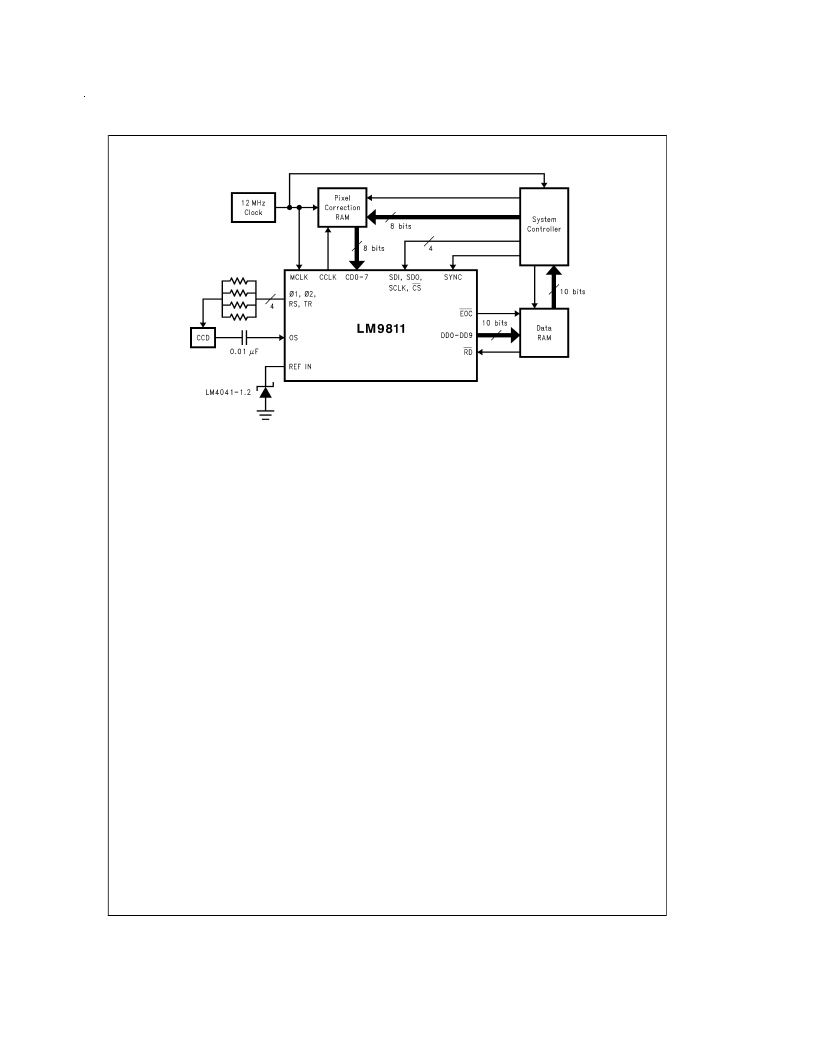
Block Diagram of LM9811-Based System
Applications Information
1.0 THEORY OF OPERATION
The LM9811 removes errors from and digitizes a linear CCD
pixel stream, while providing all the necessary clock signals
to drive the CCD. Offset and gain errors for individual pixels
are removed at the pixel rate. Offset errors are removed
through correlated double sampling (CDS). Gain errors
(which may come from any combination of PRNU, uneven il-
lumination, cos
4
effect, RGB filter mismatch, etc.) are re-
moved through the use of a 8-bit programmable gain ampli-
fier (PGA) in front of the ADC.
1.1 The Analog Signal Path
(See Block Diagram)
The analog output signal from the CCD is connected to the
OS Input of the LM9811 through a 0.01 μF (typical, see Sec-
tion 4.2, Clamp Capacitor Selection ) DC blocking capacitor.
During the CCD’s optical black pixel segment at the begin-
ning of every line, this input is clamped to the REF OUT
voltage (approximately 2.45V). This DC restore operation
fixes the reference level of the CCD pixel stream at REF
OUT
MID
.
The signal is then buffered and fed to a digitally-programmed
4-bit VGA (variable gain amplifier). The gain of the VGA is
digitally programmable in 16 steps from 1V/V to 3V/V. The
VGAis used to compensate for peak white CCD outputs less
than the 1.225V full-scale required by the LM9811 for maxi-
mum dynamic range. When used with parallel output CCDs,
the VGA can fine-tune the amplitude of the red, green, and
blue signals. For a detailed explanation of the VGA, see Sec-
tion 4.3.
The output of the VGAgoes into the CDS (Correlated Double
Sampling) stage, consisting of two sample/hold amplifiers:
S/H Ref (Reference) and S/H Signal. The reference level of
the signal is sampled and held by the S/H Ref circuit and the
active pixel data is sampled and held by the S/H Signal cir-
cuit. The output of S/H Ref is subtracted from the S/H Signal
output and amplified by 2. The full-scale signal range at this
point is approximately 2.45Vp-p. CDS reduces or eliminates
many sources of noise, including reset noise, flicker noise,
and both high and low frequency pixel-to-pixel offset varia-
tion. For more information on the CDS stage, see Section
4.4.
At this point an offset voltage can be injected by the 5-bit (4
bits + sign) Offset DAC. This voltage is designed to compen-
sate for any small fixed DC offset introduced by the CDS
S/Hs and the x2 amplifier. The LSB size of the DAC is ap-
proximately 1.7 ADC LSBs (4 mV). The adjustment range is
±
25 ADC LSBs. For a detailed explanation of the Offset
DAC, see Section 4.6.
The next stage is the PGA. This is a programmable gain am-
plifier that changes the gain at the pixel rate to correct for
gain errors due to PRNU, uneven illumination (such as cos
4
effect), RGB filter mismatch, etc. The gain adjustment range
is 0 dB to 9 dB (1V/V to 3V/V) with 8 bits of resolution. The
gain data (correction coefficients) is provided on the
CD0–CD7 bus. The gain may also be fixed at any value be-
tween 0 dB and 9 dB with the
PGA Gain Coefficient
con-
figuration register. For additional information on the PGA,
see Section 4.7.
An approximately 8 LSB (19 mV) offset can be added at the
output of the PGAstage if necessary to ensure that the offset
is greater than zero. This eliminates the possibility of a nega-
tive offset clipping the darkest output pixels. For more infor-
mation on the Offset Add Bit, see Section 4.8.
Finally, the output of the PGA is digitized by the ADC and
made available on the DD0–DD9 bus (Section 4.9).
Three reference voltages are used throughout the signal
path: the externally supplied REF IN (1.225V), and the inter-
nally generated REF OUT
MID
(2.45V) and REF OUT
HI
(3.675V).
DS012813-28
Power supplies and bypass capacitors not shown for clarity.
FIGURE 20. LM9811 System Block Diagram
www.national.com
21
相關PDF資料 |
PDF描述 |
|---|---|
| LM9831CCVJD | LM9831 42-Bit Color, 1200dpi USB Image Scanner |
| LM9831 | LM9831 42-Bit Color, 1200dpi USB Image Scanner |
| LM9831CCVJDX | LM9831 42-Bit Color, 1200dpi USB Image Scanner |
| LM9832CCVJD | LM9832 42-Bit Color, 1200dpi USB Image Scanner |
| LM9832 | LM9832 42-Bit Color, 1200dpi USB Image Scanner |
相關代理商/技術參數(shù) |
參數(shù)描述 |
|---|---|
| LM9811CCVF | 制造商:NSC 制造商全稱:National Semiconductor 功能描述:10-Bit Greyscale/30-Bit Color Linear CCD Sensor Processor |
| LM9812 | 制造商:NSC 制造商全稱:National Semiconductor 功能描述:LM9812 30-Bit Color Linear CCD Sensor Processor |
| LM9812CCV | 制造商:NSC 制造商全稱:National Semiconductor 功能描述:LM9812 30-Bit Color Linear CCD Sensor Processor |
| LM981-SC36 | 功能描述:基本/快動開關 Foot Switch RoHS:否 制造商:Omron Electronics 觸點形式:SPDT 執(zhí)行器:Lever 電流額定值:5 A 電壓額定值 AC:250 V 電壓額定值 DC:30 V 功率額定值: 工作力:120 g IP 等級:IP 67 NEMA 額定值: 端接類型:Wire 安裝:Panel |
| LM981-ZZ | 功能描述:基本/快動開關 Foot Switch RoHS:否 制造商:Omron Electronics 觸點形式:SPDT 執(zhí)行器:Lever 電流額定值:5 A 電壓額定值 AC:250 V 電壓額定值 DC:30 V 功率額定值: 工作力:120 g IP 等級:IP 67 NEMA 額定值: 端接類型:Wire 安裝:Panel |
發(fā)布緊急采購,3分鐘左右您將得到回復。