- 您現(xiàn)在的位置:買(mǎi)賣(mài)IC網(wǎng) > PDF目錄361035 > LM9800 (National Semiconductor Corporation) 8-Bit Greyscale/24-Bit Color Linear CCD Sensor Processor PDF資料下載
參數(shù)資料
| 型號(hào): | LM9800 |
| 廠商: | National Semiconductor Corporation |
| 英文描述: | 8-Bit Greyscale/24-Bit Color Linear CCD Sensor Processor |
| 中文描述: | 8位Greyscale/24-Bit彩色線陣CCD傳感器處理器 |
| 文件頁(yè)數(shù): | 31/34頁(yè) |
| 文件大?。?/td> | 619K |
| 代理商: | LM9800 |
第1頁(yè)第2頁(yè)第3頁(yè)第4頁(yè)第5頁(yè)第6頁(yè)第7頁(yè)第8頁(yè)第9頁(yè)第10頁(yè)第11頁(yè)第12頁(yè)第13頁(yè)第14頁(yè)第15頁(yè)第16頁(yè)第17頁(yè)第18頁(yè)第19頁(yè)第20頁(yè)第21頁(yè)第22頁(yè)第23頁(yè)第24頁(yè)第25頁(yè)第26頁(yè)第27頁(yè)第28頁(yè)第29頁(yè)第30頁(yè)當(dāng)前第31頁(yè)第32頁(yè)第33頁(yè)第34頁(yè)
Applications Information
(Continued)
All 4 digital outputs (
φ
1,
φ
2, RS, and TR) are enabled. The
TR pulse width is set to the minimum, 20 MCLKs, as is the
guardband between
φ
1 and TR. Either of these settings can
be increased if necessary.
The TR polarity is positive, as is the RS polarity. Some CCDs
may require one or both of these signals to be inverted, in
which case the corresponding bit can be set to a “1”. If there
is an inverting buffer between the LM9800 and the CCD,
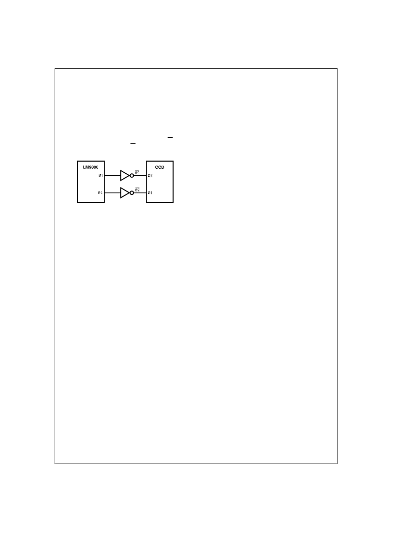
these bits can be also used to correct the output polarity at
the CCD. Note that if
φ
1 and
φ
2 are inverted, then
φ
2 should
be used as
φ
1 at the CCD, and
φ
1 should be used as
φ
2 at
the CCD (Figure 44).
The number of dummy pixels and optical black reference
pixels are given in the CCD’s datasheet. The dummy pixel
register should be programmed with the number of dummy
pixels in the CCD + 1 (for example, if the CCD has 16
dummy pixels then the register should contain 17). The opti-
cal black reference register should be programmed with the
number of optical black pixels in the CCD.
The PGA gain coefficient register and PGA Gain Source bit
are used during calibration (see section 6.0). The Power
Down bit should be set to 0 for normal operation. The Offset
Add bit is also programmed durIng calibration.
The VGA settings should be all zeros (0 0 0 0) if the VGA is
not going to be used, or all ones (1 1 1 1) if the VGA will be
used to provide additional input signal gain. If using a se-
quential color CCD, see section 4.4).
The Offset DAC bits are programmed during calibration (sec-
tion 6.0). The Test Mode bits should always be set to “0”.
9.0 HINTS AND COMMON SYSTEM DESIGN
PROBLEMS
9.1 Reading and Writing to the Configuration Register
The Configuration Register sends and receives data LSB
(Least Significant Byte) first. Some microcontrollers send out
data MSB (Most Significant Byte) first.
The SYNC pin must be high to send/receive data to/from the
Configuration Register.
9.2 Examine the CCLK and EOC Timing
As explained earlier, this timing depends on the position of
the Sample Reference (SR) pulse, and for some values of
SR it is not what you would expect. Pay close attention to
Timing Diagrams (Figures 23, 24, 25, 26).
9.3 Setting the Dummy and Optical Black Pixel
Registers
The minimum value in the Dummy Pixels register is 1. Note
that the value in this register should be equal to 1 plus the
actual number of dummy pixels in the CCD. For example, if
the CCD being used with the LM9800 has 12 dummy pixels,
this register should be set to 13. The minimum number in the
Optical Black Pixels register is 1.
DS012498-52
FIGURE 44.
φ
1 and
φ
2 After Inversion
31
www.national.com
相關(guān)PDF資料 |
PDF描述 |
|---|---|
| LM9800CCV | 8-Bit Greyscale/24-Bit Color Linear CCD Sensor Processor |
| LM9811CCVF | 10-Bit Greyscale/30-Bit Color Linear CCD Sensor Processor |
| LM9811 | 10-Bit Greyscale/30-Bit Color Linear CCD Sensor Processor |
| LM9811CCV | 10-Bit Greyscale/30-Bit Color Linear CCD Sensor Processor |
| LM9831CCVJD | LM9831 42-Bit Color, 1200dpi USB Image Scanner |
相關(guān)代理商/技術(shù)參數(shù) |
參數(shù)描述 |
|---|---|
| LM9800CCV | 制造商:NSC 制造商全稱(chēng):National Semiconductor 功能描述:8-Bit Greyscale/24-Bit Color Linear CCD Sensor Processor |
| LM9800CCVF | 制造商:未知廠家 制造商全稱(chēng):未知廠家 功能描述:Special Function Video Processor |
| LM9801 | 制造商:NSC 制造商全稱(chēng):National Semiconductor 功能描述:Greyscale/24-Bit Color Linear CCD Sensor Processor |
| LM9801CCV | 制造商:NSC 制造商全稱(chēng):National Semiconductor 功能描述:Greyscale/24-Bit Color Linear CCD Sensor Processor |
| LM9801CCVF | 制造商:NSC 制造商全稱(chēng):National Semiconductor 功能描述:Greyscale/24-Bit Color Linear CCD Sensor Processor |
發(fā)布緊急采購(gòu),3分鐘左右您將得到回復(fù)。