- 您現(xiàn)在的位置:買賣IC網(wǎng) > PDF目錄361035 > LM9800 (National Semiconductor Corporation) 8-Bit Greyscale/24-Bit Color Linear CCD Sensor Processor PDF資料下載
參數(shù)資料
| 型號: | LM9800 |
| 廠商: | National Semiconductor Corporation |
| 英文描述: | 8-Bit Greyscale/24-Bit Color Linear CCD Sensor Processor |
| 中文描述: | 8位Greyscale/24-Bit彩色線陣CCD傳感器處理器 |
| 文件頁數(shù): | 24/34頁 |
| 文件大小: | 619K |
| 代理商: | LM9800 |
第1頁第2頁第3頁第4頁第5頁第6頁第7頁第8頁第9頁第10頁第11頁第12頁第13頁第14頁第15頁第16頁第17頁第18頁第19頁第20頁第21頁第22頁第23頁當(dāng)前第24頁第25頁第26頁第27頁第28頁第29頁第30頁第31頁第32頁第33頁第34頁
Applications Information
(Continued)
For maximum system reliability, each configuration register
location can be read back and verified after a write.
If the serial I/O to the configuration register falls out of sync
for any reason, it can be reset by a rising edge on the SYNC
pin input.
2.2 Writing Correction Coefficient Data on the
CD0–CD6 Bus
Correction coefficient data for each pixel is latched on the
rising edge of the CCLK output signal (see Figure 10). Note
that there is a 4 pixel latency between when the coefficient
data is latched and when the output data is available.As Fig-
ure 2
Pixel Pipeline Timing Overview
shows, coefficient
data for pixel n is latched shortly before the output data for
pixel n-2 becomes available on the output databus
(DD0–DD7). Figures 23, 24, 25, 26show the timing for coef-
ficient data and output data at the beginning of each line.
Note that there is no way to provide a correction coefficient
for pixel 1, the first pixel in the CCD array. This is usually not
a problem since the first several pixels of most CCDs are not
used. The timing at the beginning of a line is discussed in de-
tail in section 2.4.
2.3 Reading Output Data on the DD0–DD7 Bus
The corrected digital output data representing each pixel is
available on the DD0–DD7 databus. The data is valid after
the falling edge of the EOC output. The RD input takes the
databus in and out of TRI-STATE. RD can be held low at all
times if there are no other devices needing the bus, or it can
be used to TRI-STATE the bus between pixels, allowing
other devices access to the bus. Figure 12 shows how EOC
can be tied to RD to automatically multiplex between coeffi-
cient data and conversion data.
2.4 EOC and CCLK at Startup
At the beginning of every line, the LM9800 internally syn-
chronizes
the
EOC
and
user-programmed sample periods. The timing of EOC and
CCLK during this adjustment period depends on the settings
in the
RS Pulse Position
(RS) and
Sample Reference Po-
sition
(SR) registers, as shown in Figures 23, 24, 25, 26
The numbers inside the CCLK and EOC signals indicate the
width (in MCLK periods) of that signal while it is in that state.
The EOC and CCLK pulse train is synchronized with the po-
sition of the Sample Reference pulse. For most RS and SR
combinations (shown in table and timing of Figure 23), in-
creasing SR simply stretches out the second EOC and
CCLK cycle. When SR is greater than 10 (typically with
even/odd CCDs), the timing gets more complex, and should
be considered when building any systems that rely on the
EOC and/or CCLK signals for counting, or expect them to
never be low simultaneously.
CCLK
signals
with
the
2.5 MCLK
This is the master clock input that controls the LM9800. The
pixel conversion rate is fixed at 1/8 of this frequency. Many of
the timing parameters are also relative to the frequency of
this clock.
2.6 SYNC
This input signals the beginning of a line. When SYNC goes
high, the LM9800 generates a TR pulse, then begins con-
verting pixels until the SYNC line is brought low again. Since
there is no pixel counter in the LM9800, it will work with
CCDs of any length.
SYNC must be high to read from or write to the Configuration
Register. The rising edge of SYNC resets the serial I/O’s in-
ternal shift register, so any noise or sporadic signals on the
SCLK input prior to SYNC going high will be ignored.
3.0 DIGITAL CCD INTERFACE
3.1 Buffering
φ
1,
φ
2, RS, and TR
The LM9800 can drive the
φ
1,
φ
2, RS, and TR inputs of
many CCDs directly, without the need for external buffers be-
tween the LM9800 and the CCD. Most linear CCDs de-
signed for scanner applications require 0V to 5V signal
swings into 20pF to 500pF input loading. Series resistors are
typically inserted between the driver and the CCD to control
slew rate and isolate the driver from the large load capaci-
tances. The values of these resistors are usually given in the
CCD’s datasheet.
4.0 ANALOG INTERFACE
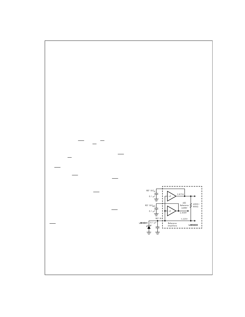
4.1 Voltage Reference
The two REF IN pins should be connected to a 1.225V
±
2%
reference voltage capable of sinking between 2mA and 8mA
of current coming from the 400
–900
resistor string be-
tween REF OUT
and REF IN. The LM4041-1.2 1.225V
bandgap reference is recommended for this application as
shown in Figure 28 The inexpensive “E” grade meets all the
requirements of the application and is available in a TO-92
(LM4041EIZ-1.2) package as well as a SOT-23 package
(LM4041EIM3-1.2) to minimize board space.
Due to the transient currents generated by the LM9800’s
ADC, PGA, and CDS circuitry, the REF IN pins, the REF
OUT
pin and the REF OUT
pin should all be bypassed
to AGND with 0.1μF monolithic capacitors.
4.2 Clamp Capacitor Selection
The output signal of most CCDs rides on a large DC offset
(typically 8V to 10V) which is incompatible with the LM9800’s
5V operation. To eliminate this offset without resorting to ad-
ditional higher voltage components, the output of the CCD is
AC coupled to the LM9800 through a DC blocking capacitor,
C
(the CCD’s DOS output is not used). The value of
this capacitor is determined by the leakage current of the
DS012498-34
FIGURE 28. Voltage Reference Generation
www.national.com
24
相關(guān)PDF資料 |
PDF描述 |
|---|---|
| LM9800CCV | 8-Bit Greyscale/24-Bit Color Linear CCD Sensor Processor |
| LM9811CCVF | 10-Bit Greyscale/30-Bit Color Linear CCD Sensor Processor |
| LM9811 | 10-Bit Greyscale/30-Bit Color Linear CCD Sensor Processor |
| LM9811CCV | 10-Bit Greyscale/30-Bit Color Linear CCD Sensor Processor |
| LM9831CCVJD | LM9831 42-Bit Color, 1200dpi USB Image Scanner |
相關(guān)代理商/技術(shù)參數(shù) |
參數(shù)描述 |
|---|---|
| LM9800CCV | 制造商:NSC 制造商全稱:National Semiconductor 功能描述:8-Bit Greyscale/24-Bit Color Linear CCD Sensor Processor |
| LM9800CCVF | 制造商:未知廠家 制造商全稱:未知廠家 功能描述:Special Function Video Processor |
| LM9801 | 制造商:NSC 制造商全稱:National Semiconductor 功能描述:Greyscale/24-Bit Color Linear CCD Sensor Processor |
| LM9801CCV | 制造商:NSC 制造商全稱:National Semiconductor 功能描述:Greyscale/24-Bit Color Linear CCD Sensor Processor |
| LM9801CCVF | 制造商:NSC 制造商全稱:National Semiconductor 功能描述:Greyscale/24-Bit Color Linear CCD Sensor Processor |
發(fā)布緊急采購,3分鐘左右您將得到回復(fù)。