- 您現(xiàn)在的位置:買賣IC網(wǎng) > PDF目錄361034 > LM78CCVF-J (NATIONAL SEMICONDUCTOR CORP) Microprocessor System Hardware Monitor PDF資料下載
參數(shù)資料
| 型號: | LM78CCVF-J |
| 廠商: | NATIONAL SEMICONDUCTOR CORP |
| 元件分類: | 模擬信號調(diào)理 |
| 英文描述: | Microprocessor System Hardware Monitor |
| 中文描述: | SPECIALTY ANALOG CIRCUIT, PQFP44 |
| 封裝: | 10 X 10 MM, PLASTIC, QFP-44 |
| 文件頁數(shù): | 3/31頁 |
| 文件大?。?/td> | 424K |
| 代理商: | LM78CCVF-J |
第1頁第2頁當(dāng)前第3頁第4頁第5頁第6頁第7頁第8頁第9頁第10頁第11頁第12頁第13頁第14頁第15頁第16頁第17頁第18頁第19頁第20頁第21頁第22頁第23頁第24頁第25頁第26頁第27頁第28頁第29頁第30頁第31頁
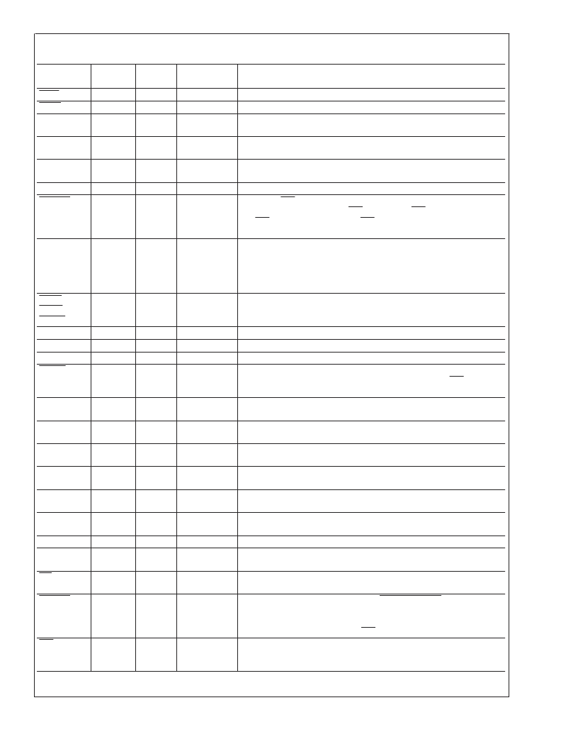
Pin Descriptions
Pin
Name(s)
IORD
IOWR
SYSCLK
Pin
Number
1
2
3
Number
of Pins
1
1
1
Type
Description
Digital Input
Digital Input
Digital Input
An active low standard ISA bus I/O Read Control.
An active low standard ISA bus I/O Write Control.
The reference clock for the ISA bus. Typically ranges from 4.167 MHz to
8.33 MHz. The minimum clock frequency this input can handle is 1 Hz.
Bi-directional ISA bus Data lines. D0 corresponds to the low order bit,
with D7 the high order bit.
+5V V
CC
power. Bypass with the parallel combination of 10 μF
(electolytic or tantalum) and 0.1 μF (ceramic) bypass capacitors.
Internally connected to all digital circuitry.
Chainable SMI (System Management Interrupt) Input. This is an active
low input that propagates the SMI signal to the SMI output of the LM78
via SMI Mask Register Bit 6 and SMI enable Bit 1 of the Configuration
Register.
An active high input from an external circuit which latches a Chassis
Intrusion event. This line can go high without any clamping action
regardless of the powered state of the LM78. The LM78 provides an
internal open drain on this line, controlled by Bit 7 of NMI Mask Register
2, to provide a minimum 20 ms reset of this line.
An active low push-pull output intended to drive an external P-channel
power MOSFET for software power control.
D7–D0
4–11
8
Digital I/O
V
CC
(+5V)
12
1
POWER
GNDD
SMI__IN
13
14
1
1
GROUND
Digital Input
Chassis
Intrusion
15
1
Digital I/O
Power
Switch
Bypass
FAN3–FAN1
SCL
SDA
RESET
16
1
Digital Output
17–19
20
21
22
3
1
1
1
Digital Input
Digital Input
Digital I/O
Digital Output
0V to +5V amplitude fan tachometer input.
Serial Bus Clock.
Serial Bus bidirectional Data.
Master Reset, 5 mA driver (open drain), active low output with a 20 ms
minimum pulse width. Available when enabeld via Bit 7 in SMI Mask
Register 2.
NAND Tree totem-pole output that provides board-level connectivity
testing. Refer to Section 11.0 on NAND Tree testing.
Internally connected to all analog circuitry. The ground reference for all
analog inputs.
Ground-referred inverting op amp input. Refer to Section 4.0, “ANALOG
INPUTS”.
Output of inverting op amp for Input 6. Refer to section 4.0, “ANALOG
INPUTS”.
Output of inverting op amp for Input 5. Refer to section 4.0, “ANALOG
INPUTS”.
Ground-referred inverting op amp input. Refer to Section 4.0, “ANALOG
INPUTS”.
0V to 4.096V FSR Analog Inputs.
Voltage Supply readouts from P6. This value is read in the VID/Fan
Divisor Register.
Board Temperature Interrupt driven by O.S. outputs of additional
temperature sensors such as LM75. Provides internal pull-up of 10 k
.
Non-Maskable Interrupt (open source)/Interrupt Request (open drain).
The mode is selected with Bit 5 of the Configuration Register and the
output is enabled when Bit 2 of the Configuration Register is set to 1.
The default state is disabled and IRQ mode.
System Management Interrupt (open drain). This output is enabled when
Bit 1 in the Configuration Register is set to 1. The default state is
disabled.
NTEST
23
1
Test Output
GNDA
24
1
GROUND
IN6
25
1
Analog Input
FB6
26
1
Analog Output
FB5
27
1
Analog Output
IN5
28
1
Analog Input
IN4–IN0
VID3–VID0
29–33
34–37
5
4
Analog Input
Digital Input
BTI
38
1
Digital Input
NMI/IRQ
39
1
Digital Output
SMI
40
1
Digital Output
L
www.national.com
3
相關(guān)PDF資料 |
PDF描述 |
|---|---|
| LM79CCVF | Microprocessor System Hardware Monitor |
| LM79 | |
| LM81CIMTX-32 | Serial Interface ACPI-Compatible Microprocessor System |
| LM81 | Serial Interface ACPI-Compatible Microprocessor System |
| LM81CIMT-31 | Serial Interface ACPI-Compatible Microprocessor System |
相關(guān)代理商/技術(shù)參數(shù) |
參數(shù)描述 |
|---|---|
| LM78D05A | 制造商:CYSTEKEC 制造商全稱:Cystech Electonics Corp. 功能描述:Three Terminal Positive Voltage Regulators |
| LM78D05AJ3 | 制造商:CYSTEKEC 制造商全稱:Cystech Electonics Corp. 功能描述:Three Terminal Positive Voltage Regulators |
| LM78D05B | 制造商:CYSTEKEC 制造商全稱:Cystech Electonics Corp. 功能描述:Three Terminal Positive Voltage Regulators |
| LM78D05BJ3 | 制造商:CYSTEKEC 制造商全稱:Cystech Electonics Corp. 功能描述:Three Terminal Positive Voltage Regulators |
| LM78D05XJ3 | 制造商:CYSTEKEC 制造商全稱:Cystech Electonics Corp. 功能描述:Three Terminal Positive Voltage Regulators |
發(fā)布緊急采購,3分鐘左右您將得到回復(fù)。