- 您現(xiàn)在的位置:買賣IC網(wǎng) > PDF目錄361030 > LM5026SDX (NATIONAL SEMICONDUCTOR CORP) Active Clamp Current Mode PWM Controller PDF資料下載
參數(shù)資料
| 型號: | LM5026SDX |
| 廠商: | NATIONAL SEMICONDUCTOR CORP |
| 元件分類: | 穩(wěn)壓器 |
| 英文描述: | Active Clamp Current Mode PWM Controller |
| 中文描述: | 3 A SWITCHING CONTROLLER, 660 kHz SWITCHING FREQ-MAX, DSO16 |
| 封裝: | 5 X 5 MM, EXPOSED PAD, LLP-16 |
| 文件頁數(shù): | 13/23頁 |
| 文件大?。?/td> | 936K |
| 代理商: | LM5026SDX |
PWM Comparator/Slope Compensation
(Continued)
For duty cycles greater than 50 percent, current mode con-
trol circuits are subject to sub-harmonic oscillation. By add-
ing an additional fixed slope voltage ramp signal (slope
compensation) to the current sense signal, this oscillation
can be avoided. The LM5026 integrates this slope compen-
sation by summing a current ramp generated by the oscilla-
tor with the current sense signal. The PWM comparator
ramp signal is a combination of the current waveform at the
CS pin, and an internally generated slope compensation
ramp derived from the oscillator. The internal ramp has an
amplitude of 0 to 45 μAwhich is sourced into an internal 2 k
resistor, plus the external impedance at the CS pin. Addi-
tional slope compensation may be added by increasing the
source impedance of the current sense signal.
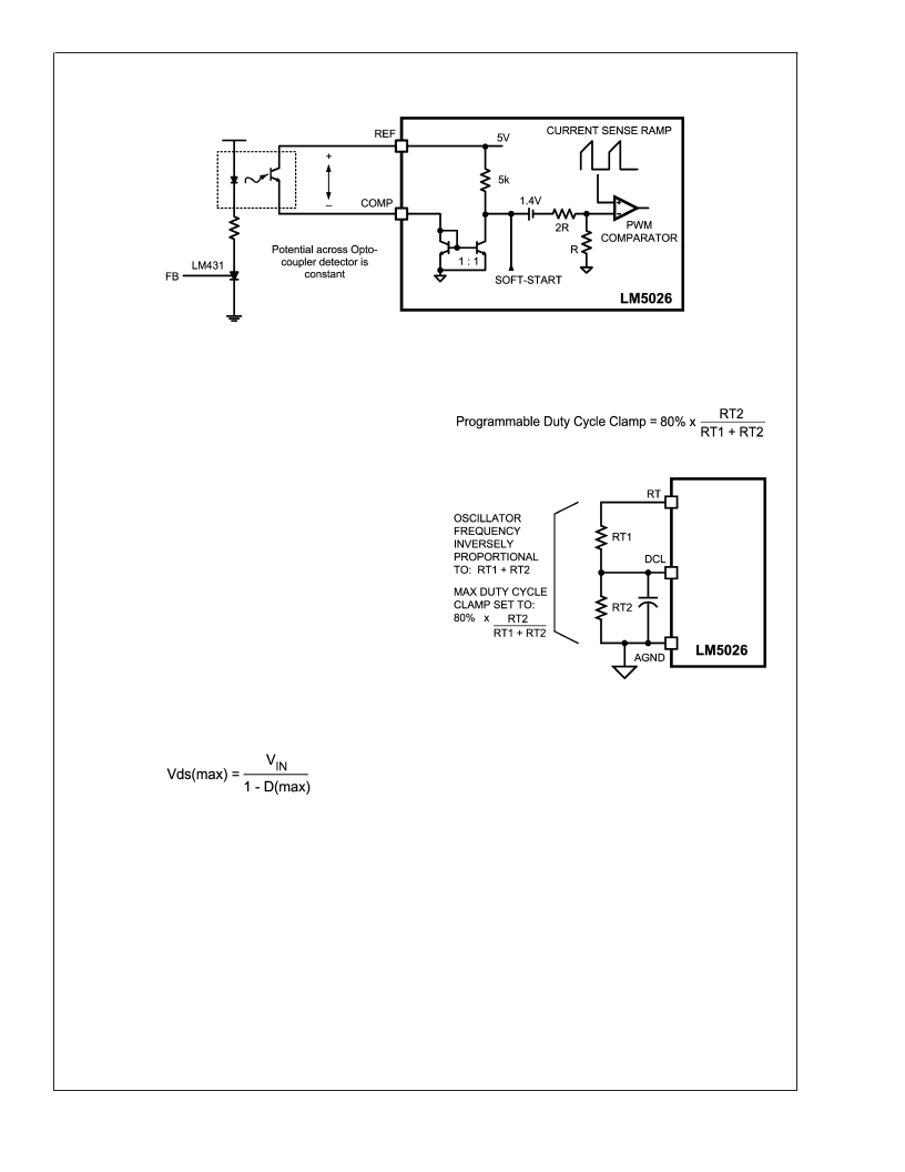
Maximum Duty Cycle Clamp
Controlling the maximum duty cycle of an active clamp reset
PWM controller is necessary to limit the voltage stress on the
main and active clamp MOSFETs. The relationship between
the maximum drain-source voltage of the MOSFETs and the
maximum PWM duty cycle is provided by the following equa-
tion:
The main output (OUT_A) duty cycle is normally controlled
by the control current sourced into the COMP pin from the
external feedback circuit. When the feedback demands
maximum output from the converter, the duty cycle will be
limited by one of two circuits within the LM5026: the user
programmable duty cycle clamp and the voltage-dependent
duty cycle limiter, which varies inversely with the input line
voltage.
Programmable Duty Cycle Clamp – The maximum allowed
duty cycle can be programmed by setting a voltage at the
DCL pin to a value less than 2V. The recommended method
to set the DCL pin voltage is with a resistor divider connected
from the RT pin to AGND. The voltage at the RT pin is
internally regulated to 2V, while the current sourced from the
RT pin sets the oscillator frequency. The maximum duty can
be programmed, according to the following equation:
Line Voltage Duty Cycle Limiter - The maximum duty cycle
for the main output driver is also limited by the voltage at the
UVLO pin, which is normally proportional to VIN. The con-
troller outputs are disabled until the UVLO pin voltage ex-
ceeds 1.25V.At the minimum operating voltage (when UVLO
= 1.25V) the maximum duty cycle starts at the duty cycle
clamp level programmed by the DCL pin voltage (80% or
less). As the line voltage increases, the maximum duty cycle
decreases linearly with increasing UVLO voltage, as illus-
trated in
Figure 6
. Ultimately the duty cycle of the main
output is controlled to the least of the following three vari-
ables: the duty cycle controlled by the PWM comparator, the
programmable maximum duty cycle clamp, or the line volt-
age dependent duty cycle limiter.
20147915
FIGURE 4. Opto-coupler to LM5026 COMP Interface
20147916
FIGURE 5. Programming oscillator Frequency and
Maximum Duty Cycle Clamp
L
www.national.com
13
相關(guān)PDF資料 |
PDF描述 |
|---|---|
| LM5030 | 100V Push-Pull Current Mode PWM Controller |
| LM5030MM | 100V Push-Pull Current Mode PWM Controller |
| LM5030MMX | 100V Push-Pull Current Mode PWM Controller |
| LM556 | Dual Timer |
| LM556ICN | Analog Timer Circuit |
相關(guān)代理商/技術(shù)參數(shù) |
參數(shù)描述 |
|---|---|
| LM5026SDX/NOPB | 功能描述:電流型 PWM 控制器 RoHS:否 制造商:Texas Instruments 開關(guān)頻率:27 KHz 上升時間: 下降時間: 工作電源電壓:6 V to 15 V 工作電源電流:1.5 mA 輸出端數(shù)量:1 最大工作溫度:+ 105 C 安裝風格:SMD/SMT 封裝 / 箱體:TSSOP-14 |
| LM5027 | 制造商:NSC 制造商全稱:National Semiconductor 功能描述:Voltage Mode Active Clamp Controller |
| LM5027A | 制造商:NSC 制造商全稱:National Semiconductor 功能描述:Evaluation Board evaluation board is designed to provide |
| LM5027A-EVAL/NOPB | 功能描述:電源管理IC開發(fā)工具 LM5027A EVAL BRD RoHS:否 制造商:Maxim Integrated 產(chǎn)品:Evaluation Kits 類型:Battery Management 工具用于評估:MAX17710GB 輸入電壓: 輸出電壓:1.8 V |
| LM5027AMH/NOPB | 功能描述:電壓模式 PWM 控制器 Active Clamp Pwm W/3A Sr Drv RoHS:否 制造商:Texas Instruments 輸出端數(shù)量:1 拓撲結(jié)構(gòu):Buck 輸出電壓:34 V 輸出電流: 開關(guān)頻率: 工作電源電壓:4.5 V to 5.5 V 電源電流:600 uA 最大工作溫度:+ 125 C 最小工作溫度:- 40 C 封裝 / 箱體:WSON-8 封裝:Reel |
發(fā)布緊急采購,3分鐘左右您將得到回復。