- 您現(xiàn)在的位置:買賣IC網(wǎng) > PDF目錄385480 > LM3224MMX-ADJ (NATIONAL SEMICONDUCTOR CORP) 615kHz/1.25MHz Step-up PWM DC/DC Converter PDF資料下載
參數(shù)資料
| 型號: | LM3224MMX-ADJ |
| 廠商: | NATIONAL SEMICONDUCTOR CORP |
| 元件分類: | 穩(wěn)壓器 |
| 英文描述: | 615kHz/1.25MHz Step-up PWM DC/DC Converter |
| 中文描述: | 2.8 A SWITCHING REGULATOR, 1500 kHz SWITCHING FREQ-MAX, PDSO8 |
| 封裝: | PLASTIC, MSOP-8 |
| 文件頁數(shù): | 10/18頁 |
| 文件大小: | 920K |
| 代理商: | LM3224MMX-ADJ |
Operation
(Continued)
INTRODUCTION TO COMPENSATION
The LM3224 is a current mode PWM boost converter. The
signal flow of this control scheme has two feedback loops,
one that senses switch current and one that senses output
voltage.
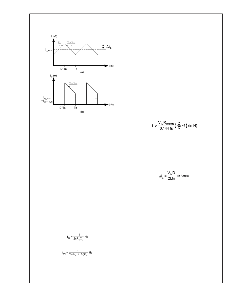
To keep a current programmed control converter stable
above duty cycles of 50%, the inductor must meet certain
criteria. The inductor, along with input and output voltage,
will determine the slope of the current through the inductor
(see
Figure 2
(a)). If the slope of the inductor current is too
great, the circuit will be unstable above duty cycles of 50%.
A 10μH to 15μH inductor is recommended for most 615 kHz
applications, while a 4.7μH to 10μH inductor may be used for
most 1.25 MHz applications. If the duty cycle is approaching
the maximum of 85%, it may be necessary to increase the
inductance by as much as 2X. See
Inductor and Diode
Selection
for more detailed inductor sizing.
The LM3224 provides a compensation pin (V
) to customize
the voltage loop feedback. It is recommended that a series
combination of R
and C
be used for the compensation
network, as shown in the typical application circuit. For any
given application, there exists a unique combination of R
C
and C
that will optimize the performance of the LM3224
circuit in terms of its transient response. The series combi-
nation of R
and C
introduces a pole-zero pair according to
the following equations:
where R
is the output impedance of the error amplifier,
approximately 900k
. For most applications, performance
can be optimized by choosing values within the range 5k
≤
R
C
≤
100k
(R
C
can be up to 200k
if C
C2
is used, see
High
Output Capacitor ESR Compensation
) and 680pF
≤
C
≤
10nF. Refer to the
Applications Information
section for rec-
ommended values for specific circuits and conditions. Refer
to the
Compensation
section for other design requirement.
COMPENSATION
This section will present a general design procedure to help
insure a stable and operational circuit. The designs in this
datasheet are optimized for particular requirements. If differ-
ent conversions are required, some of the components may
need to be changed to ensure stability. Below is a set of
general guidelines in designing a stable circuit for continu-
ous conduction operation, in most all cases this will provide
for stability during discontinuous operation as well. The
power components and their effects will be determined first,
then the compensation components will be chosen to pro-
duce stability.
INDUCTOR AND DIODE SELECTION
Although the inductor sizes mentioned earlier are fine for
most applications, a more exact value can be calculated. To
ensure stability at duty cycles above 50%, the inductor must
have some minimum value determined by the minimum
input voltage and the maximum output voltage. This equa-
tion is:
where fs is the switching frequency, D is the duty cycle, and
R
is the ON resistance of the internal switch taken from
the graph "NMOS R
vs. Input Voltage" in the
Typical
Performance Characteristics
section. This equation is only
good for duty cycles greater than 50% (D
>
0.5), for duty
cycles less than 50% the recommended values may be
used. The corresponding inductor current ripple as shown in
Figure 2
(a) is given by:
The inductor ripple current is important for a few reasons.
One reason is because the peak switch current will be the
average inductor current (input current or I
/D’) plus
i
L
.
As a side note, discontinuous operation occurs when the
inductor current falls to zero during a switching cycle, or
i
L
is greater than the average inductor current. Therefore, con-
tinuous conduction mode occurs when
i
is less than the
average inductor current. Care must be taken to make sure
that the switch will not reach its current limit during normal
operation. The inductor must also be sized accordingly. It
should have a saturation current rating higher than the peak
inductor current expected. The output voltage ripple is also
affected by the total ripple current.
The output diode for a boost regulator must be chosen
correctly depending on the output voltage and the output
current. The typical current waveform for the diode in con-
tinuous conduction mode is shown in
Figure 2
(b). The diode
must be rated for a reverse voltage equal to or greater than
the output voltage used. The average current rating must be
greater than the maximum load current expected, and the
peak current rating must be greater than the peak inductor
current. During short circuit testing, or if short circuit condi-
tions are possible in the application, the diode current rating
20097605
FIGURE 2. (a) Inductor current. (b) Diode current.
L
www.national.com
10
相關(guān)PDF資料 |
PDF描述 |
|---|---|
| LM3310 | Step-up PWM DC/DC Converter with Integrated Op-Amp and Gate Pulse Modulation Switch |
| LM3310SQ | Step-up PWM DC/DC Converter with Integrated Op-Amp and Gate Pulse Modulation Switch |
| LM3310SQX | Step-up PWM DC/DC Converter with Integrated Op-Amp and Gate Pulse Modulation Switch |
| LM3351 | Switched Capacitor Voltage Converter |
| LM3351MM | Switched Capacitor Voltage Converter |
相關(guān)代理商/技術(shù)參數(shù) |
參數(shù)描述 |
|---|---|
| LM3224MMX-ADJ/NOPB | 功能描述:DC/DC 開關(guān)控制器 RoHS:否 制造商:Texas Instruments 輸入電壓:6 V to 100 V 開關(guān)頻率: 輸出電壓:1.215 V to 80 V 輸出電流:3.5 A 輸出端數(shù)量:1 最大工作溫度:+ 125 C 安裝風(fēng)格: 封裝 / 箱體:CPAK |
| LM322H | 制造商:NSC 制造商全稱:National Semiconductor 功能描述:Precision Timers |
| LM322N | 制造商:NSC 制造商全稱:National Semiconductor 功能描述:Precision Timers |
| LM322N/B+ | 制造商:未知廠家 制造商全稱:未知廠家 功能描述:Analog Timer Circuit |
| LM323 | 制造商:STMICROELECTRONICS 制造商全稱:STMicroelectronics 功能描述:Three-terminal 3 A adjustable voltage regulators |
發(fā)布緊急采購,3分鐘左右您將得到回復(fù)。