- 您現(xiàn)在的位置:買賣IC網(wǎng) > PDF目錄361024 > LM2619MTC (NATIONAL SEMICONDUCTOR CORP) 500mA Step-Down DC-DC Converter PDF資料下載
參數(shù)資料
| 型號: | LM2619MTC |
| 廠商: | NATIONAL SEMICONDUCTOR CORP |
| 元件分類: | 穩(wěn)壓器 |
| 英文描述: | 500mA Step-Down DC-DC Converter |
| 中文描述: | 1.1 A SWITCHING REGULATOR, 1000 kHz SWITCHING FREQ-MAX, PDSO14 |
| 封裝: | MO-153AB, TSSOP-14 |
| 文件頁數(shù): | 12/16頁 |
| 文件大?。?/td> | 799K |
| 代理商: | LM2619MTC |
Device Information
(Continued)
from a pulse or function generator can develop under/
overshoot as high as 10V at the end of an improperly termi-
nated cable.
OVERVOLTAGE PROTECTION
The LM2619MTC has an over-voltage comparator that pre-
vents the output voltage from rising too high when the device
is left in PWM mode under low-load conditions. When the
output voltage rises by about 100mV (
Figure 3
) over its
regulation threshold, the OVP comparator inhibits PWM op-
eration to skip pulses until the output voltage returns to the
regulation threshold. When resistor dividers are used the
OVP threshold at the output will be the value of the threshold
at the feedback pin times the resistor divider ratio. In over
voltage protection, output voltage and ripple will increase.
SHUTDOWN MODE
Setting the EN digital input pin low (
<
0.4V) places the
LM2619MTC in a 0.02μA (typ) shutdown mode. During shut-
down, the PFET switch, NFET synchronous rectifier, refer-
ence, control and bias circuitry of the LM2619MTC are
turned off. Setting EN high enables normal operation. While
turning on, soft start is activated.
EN should be set low to turn off the LM2619MTC during
system power-up and undervoltage conditions when the
supply is less than the 2.8V minimum operating voltage. The
LM2619MTC is designed for compact portable applications,
such as mobile phones. In such applications, the system
controller determines power supply sequencing. Although
the LM2619MTC is typically well behaved at low input volt-
ages, this is not guaranteed.
INTERNAL SYNCHRONOUS RECTIFICATION
While in PWM mode, the LM2619MTC uses an internal
NFET as a synchronous rectifier to reduce rectifier forward
voltage drop and associated power loss. Synchronous rec-
tification provides a significant improvement in efficiency
whenever the output voltage is relatively low compared to
the voltage drop across an ordinary rectifier diode.
The internal NFET synchronous rectifier is turned on during
the inductor current down slope during the second part of
each cycle. The synchronous rectifier is turned off prior to the
next cycle, or when the inductor current ramps to zero at light
loads. The NFET is designed to conduct through its intrinsic
body diode during transient intervals before it turns on, elimi-
nating the need for an external diode.
CURRENT LIMITING
A current limit feature allows the LM2619MTC to protect
itself and external components during overload conditions. In
PWM mode cycle-by-cycle current limit is normally used. If
an excessive load pulls the voltage at the feedback pin down
to approximately 0.7V, then the device switches to a timed
current limit mode. In timed current limit mode the internal
P-FET switch is turned off after the current comparator trips
and the beginning of the next cycle is inhibited for 2.5μs to
force the instantaneous inductor current to ramp down to a
safe value. Timed current limit mode prevents the loss of
current control seen in some products when the voltage at
the feedback pin is pulled low in serious overload conditions.
DROPOUT CONSIDERATIONS
The LM2619MTC can be used to provide fixed output volt-
ages by using external feedback resistors. The output volt-
age can be set from 1.5V to 3.6V. The internal reference
voltage for the error amplifier is 1.5V. In cases where the
output voltage is set to 2.5V or higher, the part will go into
dropout or 100% duty cycle when the input voltage gets
close to the set output voltage. Near dropout the on time of
the P-FET may exceed one PWM clock cycle and cause
higher ripple on the output for load currents greater than
300mA. This increased ripple will exist for a narrow range of
input voltages close to the 100% duty cycle and once the
input voltage goes down further the P-FET will be fully on.
See
Setting the Output Voltage
in the
Application Information
section for further details.
In dropout conditions the output voltage is V
I
(Rdc +
R
) where Rdc is the series resistance of the inductor
and R
DSON (P)
is the on resistance of the PFET.
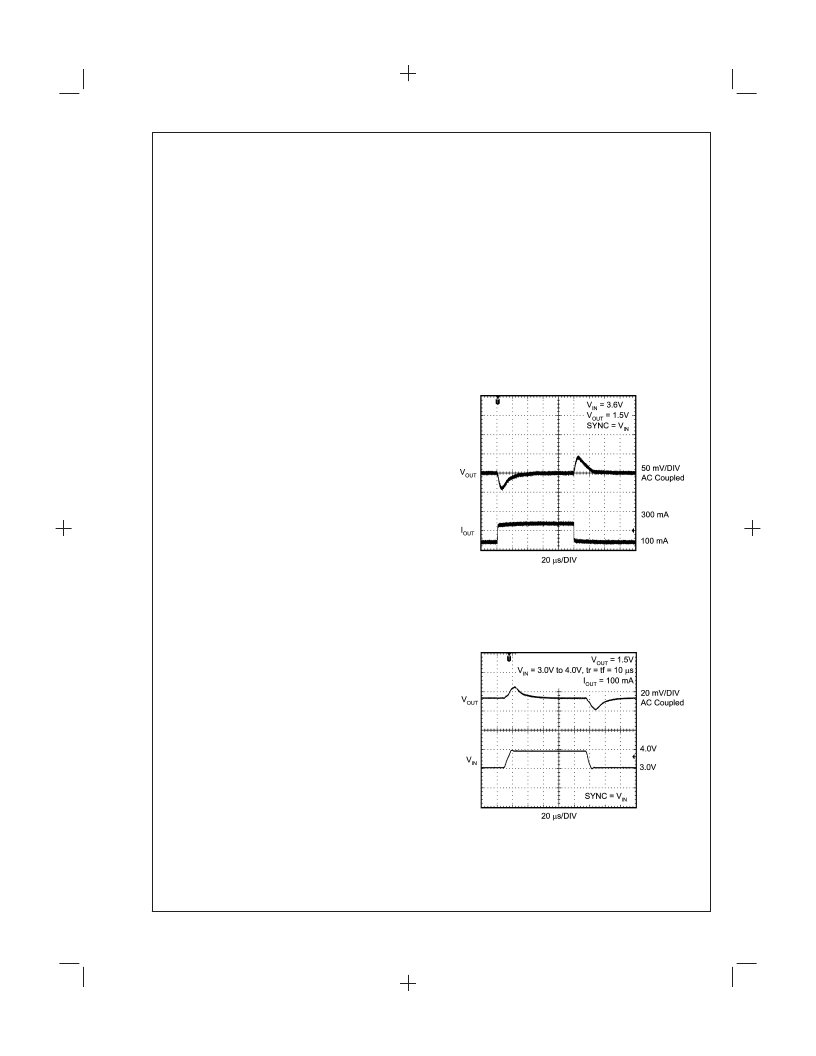
Load Transient Response
(Circuit in
Figure 3
)
20065127
FIGURE 8.
Line Transient Response
(Circuit in
Figure 3
)
20065128
FIGURE 9.
L
www.national.com
12
PrintDate=2003/08/20 PrintTime=18:54:05 801627bc ds200651_p Rev. No. 1.25
cmserv
Proof
Seq=12
相關PDF資料 |
PDF描述 |
|---|---|
| LM2619MTCX | 500mA Step-Down DC-DC Converter |
| LM2621MM | Low Input Voltage, Step-Up DC-DC Converter |
| LM2621 | |
| LM2622 | |
| LM2623 | |
相關代理商/技術參數(shù) |
參數(shù)描述 |
|---|---|
| LM2619MTC/NOPB | 功能描述:IC REG BUCK SYNC ADJ 14-TSSOP RoHS:是 類別:集成電路 (IC) >> PMIC - 穩(wěn)壓器 - DC DC 開關穩(wěn)壓器 系列:- 產(chǎn)品培訓模塊:Lead (SnPb) Finish for COTS Obsolescence Mitigation Program 標準包裝:1 系列:- 類型:降壓(降壓) 輸出類型:固定 輸出數(shù):1 輸出電壓:3.3V 輸入電壓:4.5 V ~ 24 V PWM 型:- 頻率 - 開關:- 電流 - 輸出:125mA 同步整流器:無 工作溫度:-40°C ~ 85°C 安裝類型:表面貼裝 封裝/外殼:SOT-23-6 包裝:Digi-Reel® 供應商設備封裝:SOT-6 其它名稱:MAX1836EUT33#TG16DKR |
| LM2619MTCX | 制造商:NSC 制造商全稱:National Semiconductor 功能描述:500mA Step-Down DC-DC Converter |
| LM261J | 制造商:未知廠家 制造商全稱:未知廠家 功能描述:Analog Comparator |
| LM2621 | 制造商:NSC 制造商全稱:National Semiconductor 功能描述:Low Input Voltage, Step-Up DC-DC Converter |
| LM2621_05 | 制造商:NSC 制造商全稱:National Semiconductor 功能描述:Low Input Voltage, Step-Up DC-DC Converter |
發(fā)布緊急采購,3分鐘左右您將得到回復。