- 您現(xiàn)在的位置:買賣IC網(wǎng) > PDF目錄377639 > LFX1200B-4F900I (Lattice Semiconductor Corporation) The ispXPGA architecture PDF資料下載
參數(shù)資料
| 型號: | LFX1200B-4F900I |
| 廠商: | Lattice Semiconductor Corporation |
| 英文描述: | The ispXPGA architecture |
| 中文描述: | 在ispXPGA架構(gòu) |
| 文件頁數(shù): | 8/89頁 |
| 文件大小: | 941K |
| 代理商: | LFX1200B-4F900I |
第1頁第2頁第3頁第4頁第5頁第6頁第7頁當前第8頁第9頁第10頁第11頁第12頁第13頁第14頁第15頁第16頁第17頁第18頁第19頁第20頁第21頁第22頁第23頁第24頁第25頁第26頁第27頁第28頁第29頁第30頁第31頁第32頁第33頁第34頁第35頁第36頁第37頁第38頁第39頁第40頁第41頁第42頁第43頁第44頁第45頁第46頁第47頁第48頁第49頁第50頁第51頁第52頁第53頁第54頁第55頁第56頁第57頁第58頁第59頁第60頁第61頁第62頁第63頁第64頁第65頁第66頁第67頁第68頁第69頁第70頁第71頁第72頁第73頁第74頁第75頁第76頁第77頁第78頁第79頁第80頁第81頁第82頁第83頁第84頁第85頁第86頁第87頁第88頁第89頁
Lattice Semiconductor
ispXPGA Family Data Sheet
8
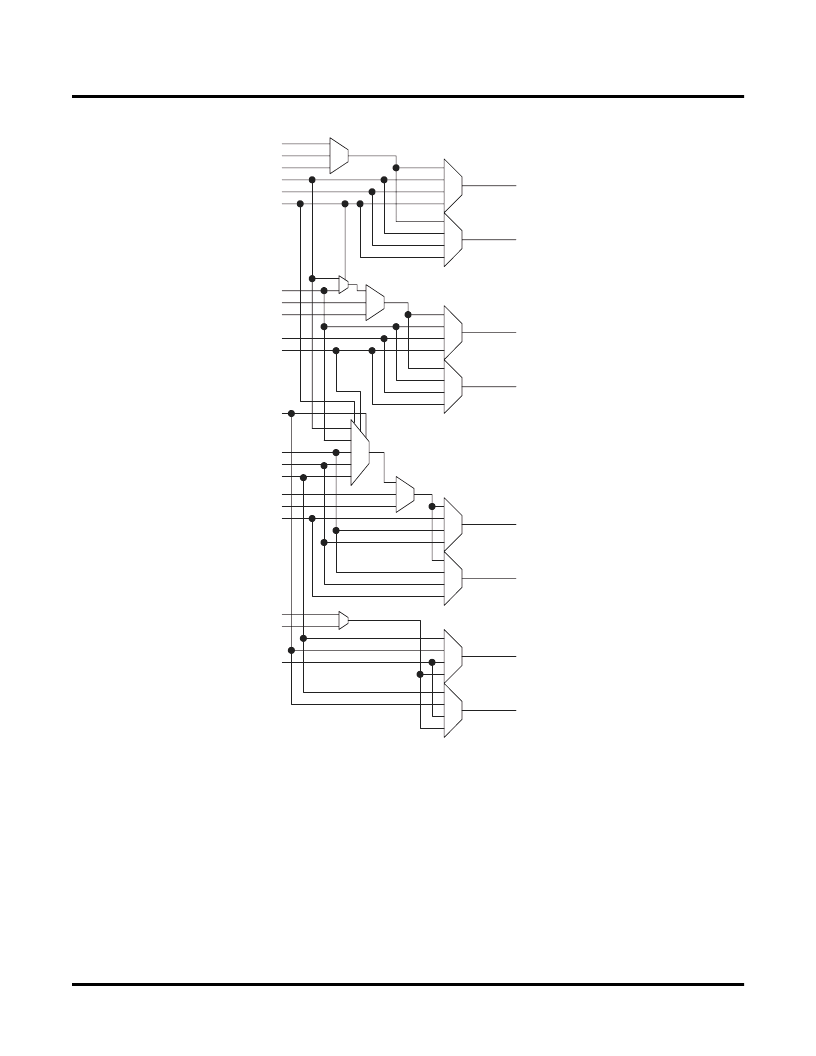
Figure 6. ispXPGA Wide Logic Generator
Con
fi
gurable Sequential Element
There are two registers in each CSE for a total of eight registers in each PFU. This high register count assists in
implementing ef
fi
cient pipelined applications with no utilization penalty. Each register can be con
fi
gured as a latch
or D type
fl
ip-
fl
op with either synchronous or asynchronous set or reset. Figure 2 shows the signals that feed the
register’s D inputs. Feed-through signals in the architecture ensure that registers are ef
fi
ciently utilized even if the
accompanying LUT is occupied.
Control Logic
The control signals available to the registers in a PFU are Clock, Clock Enable, and Set/Reset. Figure 7 shows the
various options available to generate the clock signal. As can be seen, the clock signal is the output of a 12:1 MUX
with true and compliment versions available from the 12:1 MUX. Each CSE can chose whether it uses the true or
compliment form of the clock. Figure 8 shows the Set/Reset selection for each PFU in the ispXPGA. A common
4B
XIN2
XIN3
S2
SEL1
4C
SEL2
S1
4D
S0
COUT
WIN2
WIN3
WLGW0
WLGW1
WLGX0
WLGX1
WLGY0
WLGY1
WLGZ0
WLGZ1
4A
S3
SEL0
YIN2
YIN3
ZIN2
ZIN3
SEL3
相關(guān)PDF資料 |
PDF描述 |
|---|---|
| LFX1200C-4F900I | The ispXPGA architecture |
| LFX125C-3F900I | The ispXPGA architecture |
| LFX125C-4F900I | The ispXPGA architecture |
| LFX200B-3F900I | The ispXPGA architecture |
| LFX1200B-03F900C | The ispXPGA architecture |
相關(guān)代理商/技術(shù)參數(shù) |
參數(shù)描述 |
|---|---|
| LFX1200B-4FE680C | 制造商:LATTICE 制造商全稱:Lattice Semiconductor 功能描述:ispXPGA Family |
| LFX1200B-4FE680I | 制造商:LATTICE 制造商全稱:Lattice Semiconductor 功能描述:ispXPGA Family |
| LFX1200B-4FH516C | 制造商:LATTICE 制造商全稱:Lattice Semiconductor 功能描述:ispXPGA Family |
| LFX1200B-4FH516I | 制造商:LATTICE 制造商全稱:Lattice Semiconductor 功能描述:ispXPGA Family |
| LFX1200B-4FN256C | 制造商:LATTICE 制造商全稱:Lattice Semiconductor 功能描述:ispXPGA Family |
發(fā)布緊急采購,3分鐘左右您將得到回復。