- 您現(xiàn)在的位置:買賣IC網(wǎng) > PDF目錄377635 > LFECP33E-3F256I (Lattice Semiconductor Corporation) LatticeECP/EC Family Data Sheet PDF資料下載
參數(shù)資料
| 型號(hào): | LFECP33E-3F256I |
| 廠商: | Lattice Semiconductor Corporation |
| 英文描述: | LatticeECP/EC Family Data Sheet |
| 中文描述: | LatticeECP / EC的系列數(shù)據(jù)手冊(cè) |
| 文件頁數(shù): | 17/117頁 |
| 文件大小: | 557K |
| 代理商: | LFECP33E-3F256I |
第1頁第2頁第3頁第4頁第5頁第6頁第7頁第8頁第9頁第10頁第11頁第12頁第13頁第14頁第15頁第16頁當(dāng)前第17頁第18頁第19頁第20頁第21頁第22頁第23頁第24頁第25頁第26頁第27頁第28頁第29頁第30頁第31頁第32頁第33頁第34頁第35頁第36頁第37頁第38頁第39頁第40頁第41頁第42頁第43頁第44頁第45頁第46頁第47頁第48頁第49頁第50頁第51頁第52頁第53頁第54頁第55頁第56頁第57頁第58頁第59頁第60頁第61頁第62頁第63頁第64頁第65頁第66頁第67頁第68頁第69頁第70頁第71頁第72頁第73頁第74頁第75頁第76頁第77頁第78頁第79頁第80頁第81頁第82頁第83頁第84頁第85頁第86頁第87頁第88頁第89頁第90頁第91頁第92頁第93頁第94頁第95頁第96頁第97頁第98頁第99頁第100頁第101頁第102頁第103頁第104頁第105頁第106頁第107頁第108頁第109頁第110頁第111頁第112頁第113頁第114頁第115頁第116頁第117頁
2-14
Architecture
Lattice Semiconductor
LatticeECP/EC Family Data Sheet
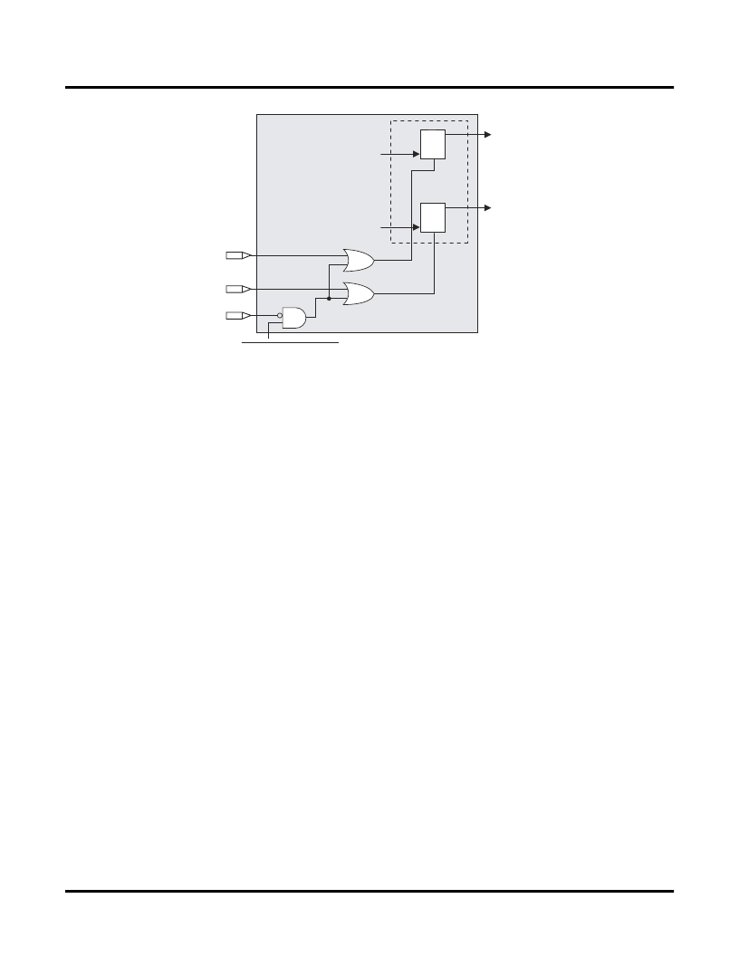
Figure 2-16. Memory Core Reset
For further information on sysMEM EBR block, please see the details of additional technical documentation at the
end of this data sheet.
sysDSP Block
The LatticeECP-DSP family provides a sysDSP block making it ideally suited for low cost, high performance Digital
Signal Processing (DSP) applications. Typical functions used in these applications are Finite Impulse Response
(FIR)
fi
lters; Fast Fourier Transforms (FFT) functions, correlators, Reed-Solomon/Turbo/Convolution encoders and
decoders. These complex signal processing functions use similar building blocks such as multiply-adders and mul-
tiply-accumulators.
sysDSP Block Approach Compare to General DSP
Conventional general-purpose DSP chips typically contain one to four (Multiply and Accumulate) MAC units with
fi
xed data-width multipliers; this leads to limited parallelism and limited throughput. Their throughput is increased by
higher clock speeds. The LatticeECP, on the other hand, has many DSP blocks that support different data-widths.
This allows the designer to use highly parallel implementations of DSP functions. The designer can optimize the
DSP performance vs. area by choosing appropriate level of parallelism. Figure 2-17 compares the serial and the
parallel implementations.
Q
SET
D
L
CLR
Output Data
Latches
Q
D
Memory Core
Port A[17:0]
SET
Port B[17:0]
RSTB
GSRN
Programmable Disable
RSTA
L
CLR
相關(guān)PDF資料 |
PDF描述 |
|---|---|
| LFEC33E-3F484C | LatticeECP/EC Family Data Sheet |
| LFECP33E-3F484C | LatticeECP/EC Family Data Sheet |
| LFEC33E-3F484I | LatticeECP/EC Family Data Sheet |
| LFECP33E-3F484I | LatticeECP/EC Family Data Sheet |
| LFEC33E-3F672C | LatticeECP/EC Family Data Sheet |
相關(guān)代理商/技術(shù)參數(shù) |
參數(shù)描述 |
|---|---|
| LFECP33E-3F484C | 功能描述:FPGA - 現(xiàn)場(chǎng)可編程門陣列 32.8K LUTs RoHS:否 制造商:Altera Corporation 系列:Cyclone V E 柵極數(shù)量: 邏輯塊數(shù)量:943 內(nèi)嵌式塊RAM - EBR:1956 kbit 輸入/輸出端數(shù)量:128 最大工作頻率:800 MHz 工作電源電壓:1.1 V 最大工作溫度:+ 70 C 安裝風(fēng)格:SMD/SMT 封裝 / 箱體:FBGA-256 |
| LFECP33E-3F484I | 功能描述:FPGA - 現(xiàn)場(chǎng)可編程門陣列 32.8K LUTs 360 I/O RoHS:否 制造商:Altera Corporation 系列:Cyclone V E 柵極數(shù)量: 邏輯塊數(shù)量:943 內(nèi)嵌式塊RAM - EBR:1956 kbit 輸入/輸出端數(shù)量:128 最大工作頻率:800 MHz 工作電源電壓:1.1 V 最大工作溫度:+ 70 C 安裝風(fēng)格:SMD/SMT 封裝 / 箱體:FBGA-256 |
| LFECP33E-3F672C | 功能描述:FPGA - 現(xiàn)場(chǎng)可編程門陣列 32.8K LUTs RoHS:否 制造商:Altera Corporation 系列:Cyclone V E 柵極數(shù)量: 邏輯塊數(shù)量:943 內(nèi)嵌式塊RAM - EBR:1956 kbit 輸入/輸出端數(shù)量:128 最大工作頻率:800 MHz 工作電源電壓:1.1 V 最大工作溫度:+ 70 C 安裝風(fēng)格:SMD/SMT 封裝 / 箱體:FBGA-256 |
| LFECP33E-3F672I | 功能描述:FPGA - 現(xiàn)場(chǎng)可編程門陣列 32.8K LUTs 496 I/O RoHS:否 制造商:Altera Corporation 系列:Cyclone V E 柵極數(shù)量: 邏輯塊數(shù)量:943 內(nèi)嵌式塊RAM - EBR:1956 kbit 輸入/輸出端數(shù)量:128 最大工作頻率:800 MHz 工作電源電壓:1.1 V 最大工作溫度:+ 70 C 安裝風(fēng)格:SMD/SMT 封裝 / 箱體:FBGA-256 |
| LFECP33E-3F900C | 制造商:LATTICE 制造商全稱:Lattice Semiconductor 功能描述:LatticeECP/EC Family Data Sheet |
發(fā)布緊急采購,3分鐘左右您將得到回復(fù)。