- 您現(xiàn)在的位置:買賣IC網(wǎng) > PDF目錄377624 > LF48410JC30 (LOGIC DEVICES INC) 1024 x 24-bit Video Histogrammer PDF資料下載
參數(shù)資料
| 型號(hào): | LF48410JC30 |
| 廠商: | LOGIC DEVICES INC |
| 元件分類: | 數(shù)字信號(hào)處理外設(shè) |
| 英文描述: | 1024 x 24-bit Video Histogrammer |
| 中文描述: | 24-BIT, DSP-HISTOGRAM PROCESSOR, PQCC84 |
| 封裝: | PLASTIC, LCC-84 |
| 文件頁數(shù): | 2/15頁 |
| 文件大?。?/td> | 302K |
| 代理商: | LF48410JC30 |
DEVICES INCORPORATED
LF48410
1024 x 24-bit Video Histogrammer
2
Video Imaging Products
08/08/2000–LDS.48410-L
SIGNAL DEFINITIONS
Power
V
CC
and GND
+5 V power supply. All pins must be
connected.
Clock
CLK — Master Clock
When operating in a synchronous
mode, the rising edge of CLK strobes
all enabled registers. CLK has no
effect when operating in an asynchro-
nous mode.
Inputs
PIN
9-0
— Pixel Data Input
PIN
9-0
provides address information
to the memory array in Histogram,
Bin Accumulate, and Look Up Table
Modes. Data is latched on the rising
edge of CLK.
DIN
23-0
— Data Input
In Bin Accumulate Mode, DIN
23-0
provides data to the internal summer
to be added to data already in the
memory array. In Look Up Table
Mode, DIN
23-0
is used to load the
memory array with the desired
values. In Delay Memory Mode, the
data to be delayed is input to the
memory array using DIN
23-0
, and in
Delay and Subtract Mode it also
provides data to be subtracted from
the delayed data. In all four modes,
DIN
23-0
is latched on the rising edge
of CLK.
IOA
9-0
— Asynchronous Address Input
IOA
9-0
provides address information
to the memory array in Asynchronous
16 and 24 Modes.
FCT
2-0
— Function Input
FCT
2-0
is used to put the LF48410 into
one of its eight modes of operation
(Table 1). Data is latched on the
rising edge of LD. To ensure proper
operation of the device, START must
be HIGH while changing modes, and
there must be at least one rising edge
of CLK between the rising edge of LD
and the falling edge of START.
Inputs/Outputs
DIO
23-0
— Data Input/Output
In all synchronous modes, DIO
23-0
is
the 24-bit registered data output port.
In all asynchronous modes, DIO
23-0
is
both the data input and data output
port for the memory array.
Controls
START — Device Enable
START is used to enable and disable
the synchronous modes of operation
(except for the Delay Memory and
Delay and Subtract Modes). The
synchronous mode sections explain
how START functions in each mode.
START has no effect in asynchronous
modes. Data is latched on the rising
edge of CLK. START must be held
HIGH when changing from one mode
to another. To ensure proper opera-
tion of the device, there must be at
least one rising edge of CLK between
the rising edge of LD and the falling
edge of START.
RD — Read/Output Enable
In all synchronous modes, RD is used
as an output enable for DIO
23-0
.
When RD is LOW, DIO
23-0
is enabled
for output. When RD is HIGH, DIO
23-0
is placed in a high-impedance state.
In all asynchronous modes, RD is
used as a read enable for the memory
array (see asynchronous mode
sections for details).
WR — Write Enable
In all asynchronous modes, WR is
used as a write enable for the
memory array (see asynchronous
mode sections for details). WR has
no effect in the synchronous modes.
UWS — Upper Word Select
UWS is only used in Asynchronous 16
Mode. If UWS is LOW and a memory
write is performed, data on DIO
15-0
is
written to the lower 16 bits of the
addressed 24-bit word. If UWS is
LOW and a memory read is per-
formed, the lower 16 bits of the
addressed 24-bit word will be output
on DIO
15-0
. If UWS is HIGH and a
memory write is performed, data on
DIO
7-0
is written to the upper 8 bits of
the addressed 24-bit word. If UWS is
HIGH and a memory read is per-
formed, the upper 8 bits of the
addressed 24-bit word will be output
on DIO
7-0
.
FC — Flash Clear
When FC is LOW, all memory array
locations and data path registers are
set to “0”. To ensure that Flash Clear
functions properly, FC should not be
set LOW until START is HIGH
(synchronous modes) or WR is HIGH
(asynchronous modes).
LD — Function Load Strobe
Data present on FCT
2-0
is latched into
the LF48410 on the rising edge of LD.
To ensure proper operation of the
device, there must be at least one
rising edge of CLK between the rising
edge of LD and the falling edge of
START.
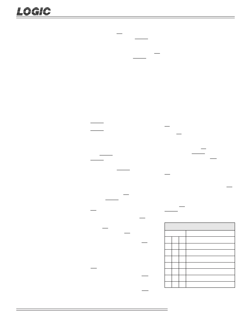
FCT
2-0
MODE
0
0
0
Histogram
0
0
1
Histogram Accumulate
0
1
0
Delay and Subtract
0
1
1
Look Up Table
1
0
0
Bin Accumulate
1
0
1
Delay Memory
1
1
0
Asynchronous 24
1
1
1
Asynchronous 16
T
ABLE
1.
LF48410 M
ODES
相關(guān)PDF資料 |
PDF描述 |
|---|---|
| LF9502 | 2K Programmable Line Buffer(2K可編程線緩沖器) |
| LF9502JC20 | 2K Programmable Line Buffer |
| LF9502JC25 | 2K Programmable Line Buffer |
| LFCN-1000 | Low Pass Filter |
| LFCN-1000D | Low Pass Filter |
相關(guān)代理商/技術(shù)參數(shù) |
參數(shù)描述 |
|---|---|
| LF48410JI25 | 制造商:未知廠家 制造商全稱:未知廠家 功能描述:Histogrammer |
| LF48410JI30 | 制造商:未知廠家 制造商全稱:未知廠家 功能描述:Histogrammer |
| LF48908 | 制造商:LOGIC 制造商全稱:LOGIC 功能描述:Two Dimensional Convolver |
| LF48908GC25 | 制造商:未知廠家 制造商全稱:未知廠家 功能描述:Video Convolver |
| LF48908GC31 | 制造商:未知廠家 制造商全稱:未知廠家 功能描述:Video Convolver |
發(fā)布緊急采購(gòu),3分鐘左右您將得到回復(fù)。