- 您現(xiàn)在的位置:買賣IC網(wǎng) > PDF目錄358760 > LC72P366 (Sanyo Electric Co.,Ltd.) On-Chip One-Time Programmable PROM Single-Chip PLL Controller PDF資料下載
參數(shù)資料
| 型號: | LC72P366 |
| 廠商: | Sanyo Electric Co.,Ltd. |
| 英文描述: | On-Chip One-Time Programmable PROM Single-Chip PLL Controller |
| 中文描述: | 片上一次性可編程可編程單芯片鎖相環(huán)控制器 |
| 文件頁數(shù): | 14/14頁 |
| 文件大小: | 154K |
| 代理商: | LC72P366 |
No. 5544-14/14
LC72P366
This catalog provides information as of November, 1996. Specifications and information herein are subject to
change without notice.
I
No products described or contained herein are intended for use in surgical implants, life-support systems, aerospace
equipment, nuclear power control systems, vehicles, disaster/crime-prevention equipment and the like, the failure of
which may directly or indirectly cause injury, death or property loss.
I
Anyone purchasing any products described or contained herein for an above-mentioned use shall:
Accept full responsibility and indemnify and defend SANYO ELECTRIC CO., LTD., its affiliates, subsidiaries and
distributors and all their officers and employees, jointly and severally, against any and all claims and litigation and all
damages, cost and expenses associated with such use:
Not impose any responsibility for any fault or negligence which may be cited in any such claim or litigation on
SANYO ELECTRIC CO., LTD., its affiliates, subsidiaries and distributors or any of their officers and employees
jointly or severally.
I
Information (including circuit diagrams and circuit parameters) herein is for example only; it is not guaranteed for
volume production. SANYO believes information herein is accurate and reliable, but no guarantees are made or implied
regarding its use or any infringements of intellectual property rights or other rights of third parties.
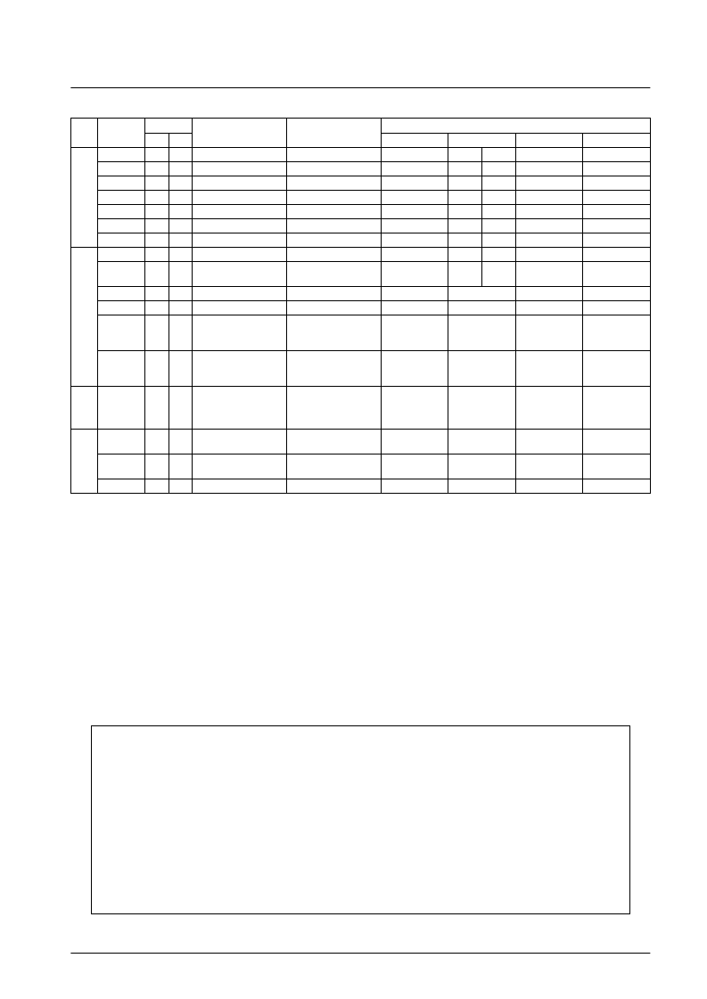
Continued from preceding page.
Mnemonic
Operand
Function
Operation
Machine code
1st
2n
D15 14
13
12
11
10
9
8
7
6
5
4
3
2
1
D0
SIO
I1
I2
Serial I/O control
SIO reg
←
I1,I2
UCCW1
←
I
UCCW2
←
I
BEEP reg
←
I
DZC reg
←
I
Timer reg
←
I
IOS reg PWn
←
N
M
←
(Pn)
Pn
←
M
0
0
0
0
0
0
0
1
I1
I2
UCS
I
Set I to UCCW1
0
0
0
0
0
0
0
0
0
0
0
1
I
UCC
I
Set I to UCCW2
0
0
0
0
0
0
0
0
0
0
1
0
I
BEEP
I
Beep control
0
0
0
0
0
0
0
0
0
1
1
0
I
DZC
I
Dead zone control
0
0
0
0
0
0
0
0
1
0
1
1
I
TMS
N
Set timer register
0
0
0
0
0
0
0
0
1
1
0
0
N
IOS
PWn
N
Set port control word
1
1
1
1
1
1
1
0
PWn
N
IN
M
Pn
Input port data to M
1
1
1
0
1
0
D
H
D
H
D
L
D
L
Pn
OUT
M
Pn
Output contents of M
to port
1
1
1
0
1
1
Pn
SPB
Pn
N
Set port bits
(Pn) N
←
1
(Pn) N
←
0
if (Pn) N = all “1”,
then skip
0
0
0
0
0
0
1
0
Pn
N
RPB
Pn
N
Reset port bits
0
0
0
0
0
0
1
1
Pn
N
TPT
Pn
N
Test port bit, then skip
if all bits specified are
true
1
1
1
1
1
1
0
0
Pn
N
TPF
Pn
N
Test port bits, then skip if (Pn) N = all “0”,
if all bits specified are
false
1
1
1
1
1
1
0
1
Pn
N
then skip
BANK
I
Select Bank
BANK
←
I
0
0
0
0
0
0
0
0
0
1
1
1
I
HALT
I
Halt mode control
HALT reg
←
I,
then CPU click stop
0
0
0
0
0
0
0
0
0
1
0
0
I
CKSTP
Clock stop
stop X’tal OSC if
HOLD = 0
0
0
0
0
0
0
0
0
0
1
0
1
NOP
No operation
No operation
0
0
0
0
0
0
0
0
0
0
0
0
H
i
I
B
i
O
i
I
g
相關(guān)PDF資料 |
PDF描述 |
|---|---|
| LC7363 | 40 AMP MINI-ISO AUTOMOTIVE RELAY |
| LC7363J | DTMF/PULSE Switchable Dialer |
| LC7363JM | DTMF/PULSE Switchable Dialer |
| LC7364 | DTMF/PULSE Switchable Dialer |
| LC7364J | DTMF/PULSE Switchable Dialer |
相關(guān)代理商/技術(shù)參數(shù) |
參數(shù)描述 |
|---|---|
| LC730Z | 制造商:SEOUL 制造商全稱:Seoul Semiconductor 功能描述:GREEN OVAL LAMP LED |
| LC731 | 制造商:SEOUL 制造商全稱:Seoul Semiconductor 功能描述:RED OVAL LAMP LED |
| LC73101C | 制造商:未知廠家 制造商全稱:未知廠家 功能描述: |
| LC73-17 | 制造商:未知廠家 制造商全稱:未知廠家 功能描述:Laser Diode with Monitor Diode |
| LC7350 | 制造商:未知廠家 制造商全稱:未知廠家 功能描述:Telecommunication IC |
發(fā)布緊急采購,3分鐘左右您將得到回復(fù)。