- 您現(xiàn)在的位置:買賣IC網(wǎng) > PDF目錄358760 > LC72P366 (Sanyo Electric Co.,Ltd.) On-Chip One-Time Programmable PROM Single-Chip PLL Controller PDF資料下載
參數(shù)資料
| 型號: | LC72P366 |
| 廠商: | Sanyo Electric Co.,Ltd. |
| 英文描述: | On-Chip One-Time Programmable PROM Single-Chip PLL Controller |
| 中文描述: | 片上一次性可編程可編程單芯片鎖相環(huán)控制器 |
| 文件頁數(shù): | 10/14頁 |
| 文件大小: | 154K |
| 代理商: | LC72P366 |
No. 5544-10/14
LC72P366
Usage Notes
The LC72P366 is provided for use in initial shipments of products designed to use the Sanyo LC72358N, LC72362N, or
LC72366. Keep the following points in mind when using this product.
Differences between the LC72P366 and the LC72358N, LC72362N, and LC72366
ROM ordering procedure when using Sanyo’s for-fee PROM programming service
— When ordering one-time programmable versions and mask versions at the same time:
The customer must provide the mask ROM version program, the mask ROM version order forms, and the one-time
programmable version order forms.
— When order just the one-time programmable version:
The customer must provide the one-time programmable version program and the one-time programmable version
order forms.
Parameter
LC72P366
LC72358N, 72362N, 72366
Operating temperature
–30 to +70C
–40 to +85C
Minimum 4.0 V
Minimum 3.5 V
CPU operating voltage
Typical
Typical
Maximum 5.5 V
Maximum 5.5 V
Minimum 3.0 V
Minimum 2.7 V
Power down detection voltage (VDET)
Typical 3.5 V
Typical 3.0 V
Maximum 4.0 V
Maximum 3.3 V
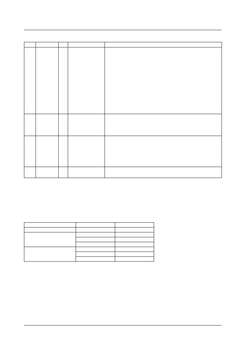
Continued from preceding page.
Pin No.
Symbol
I/O
I/O type
Function
44
43
42
41
40 to
33
32
79
2
PN0/BEEP
PN1
PN2
PN3
PO0 to PO3
PP0 to PP3
PQ0
TEST1
TEST2
O
O
I/O
CMOS push-pull
CMOS push-pull
CMOS push-pull
General-purpose output port/BEEP tone shared-function output pins
The BEEP instruction switches between the general-purpose output port and BEEP tone
functions.
General-purpose output port usage
The BEEP instruction with b3 = 0 sets up the general-purpose output port function.
Pins PN1 to PN3 are general-purpose output-only pins.
BEEP output usage
The BEEP instruction with b3 = 1 sets up BEEP output.
The BEEP instruction bits b0, b1 and b2 sets the frequency.
When set up as the BEEP port, executing an output instruction will set the internal latch
data but has no influence on the output.
These pins go to the output high-impedance state in clock stop mode.
These pins go to the output high-impedance state during the power-on reset and hold that
state until an output instruction is executed.
Output-only ports
These pins go to the output high-impedance state in clock stop mode.
These pins go to the output high-impedance state during the power-on reset and hold that
state until an output instruction is executed.
General-purpose I/O ports
The IOS instruction is used to specify input or output.
The OUTR and INR instructions are used for output and input.
The bit set, reset and test instruction cannot be used.
In clock stop mode input is disabled and these pins go to the high impedance state.
During the power-on reset, these pins function as general-purpose input ports.
LSI test pins
These pins must be either left open or connected to ground.
相關(guān)PDF資料 |
PDF描述 |
|---|---|
| LC7363 | 40 AMP MINI-ISO AUTOMOTIVE RELAY |
| LC7363J | DTMF/PULSE Switchable Dialer |
| LC7363JM | DTMF/PULSE Switchable Dialer |
| LC7364 | DTMF/PULSE Switchable Dialer |
| LC7364J | DTMF/PULSE Switchable Dialer |
相關(guān)代理商/技術(shù)參數(shù) |
參數(shù)描述 |
|---|---|
| LC730Z | 制造商:SEOUL 制造商全稱:Seoul Semiconductor 功能描述:GREEN OVAL LAMP LED |
| LC731 | 制造商:SEOUL 制造商全稱:Seoul Semiconductor 功能描述:RED OVAL LAMP LED |
| LC73101C | 制造商:未知廠家 制造商全稱:未知廠家 功能描述: |
| LC73-17 | 制造商:未知廠家 制造商全稱:未知廠家 功能描述:Laser Diode with Monitor Diode |
| LC7350 | 制造商:未知廠家 制造商全稱:未知廠家 功能描述:Telecommunication IC |
發(fā)布緊急采購,3分鐘左右您將得到回復。