- 您現(xiàn)在的位置:買賣IC網(wǎng) > PDF目錄358759 > LC72191JM (Sanyo Electric Co.,Ltd.) PLL Frequency Synthesizer for Electronic Tuning in Car Stereo Tuners PDF資料下載
參數(shù)資料
| 型號: | LC72191JM |
| 廠商: | Sanyo Electric Co.,Ltd. |
| 英文描述: | PLL Frequency Synthesizer for Electronic Tuning in Car Stereo Tuners |
| 中文描述: | 鎖相環(huán)頻率合成調(diào)諧器在汽車音響電子調(diào)諧 |
| 文件頁數(shù): | 8/16頁 |
| 文件大小: | 194K |
| 代理商: | LC72191JM |

No. 3985-8/16
LC72191, 72191M, 72191JM
No.
Control block/data
Description
Related data
(1)
(2)
(3)
(4)
Programmable divider
data
D
0
to D
15
Output port data
O
0
to O
6
General-purpose counter
initial data
CTEN
Reference frequency
data
R
0
to R
3
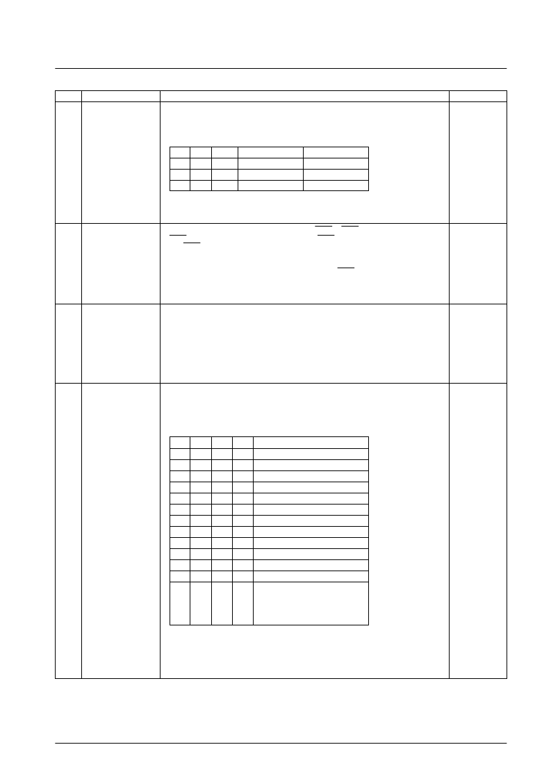
This data sets up the programmable divider.
D
0
to D
15
is a binary value with D
15
as the MSB.
The position of the LSB is changed by DV and SP as listed in the table below.
*
don’t care
When D
4
is the LSB, bits D
0
to D
3
are ignored.
Data that determines the states of the output ports OUT0 to OUT6. O
0
determines the
OUT0 pin output. However, note that when O
0
is 0, OUT0 will output a high level, and when O
0
is 1, OUT0 will output a low level. O
1
to O
6
function in the same manner.
These can be used for a wide range of purposes, including, for example, band switching
signals.
When the TB bit is set to 1, the O
0
data is ignored and the OUT0 pin outputs an 8 Hz clock
time base signal.
Since the output port states are undefined when power is first applied, transfer the control data
quickly.
Data that determines the operation of the general-purpose counter. When CTEN is 0, the 20-bit
binary counter (the general-purpose counter) is reset and the HCTR and LCTR pins are pulled
down to ground. When CTEN is set to 1, the general-purpose counter reset state is cleared and
the counter operates according to the SC bit (the general-purpose selection data). In this state,
the general-purpose counter will count either the HCTR or LCTR input signal.
Since the general-purpose counter is reset by setting CTEN to 0, the result of a count operation
must be sent to the controller while CTEN is still 1.
Data that selects one of the ten LC72191 reference frequencies or sets the LC72191 to
backup mode in which PLL operation is disabled.
Note:
*
PLL inhibit (backup mode)
The programmable divider block is turned off, both the FMIN and AMIN pins are pulled
down to ground, and the charge pump outputs go to the floating state.
DV
SP
TB
SC
SF
GT
DV
SP
LSB
Divisor setting
Actual divisor
1
*
D0
256 to 65536
Twice the set value
0
1
D0
256 to 65536
The set value
0
0
D4
4 to 4096
The set value
R
0
0
R
1
0
R
2
0
R
3
0
Reference frequency (kHz)
100
0
0
0
1
50
0
0
1
0
25
0
0
1
1
25
0
1
0
0
12.5
0
1
0
1
6.25
0
1
1
0
3.125
0
1
1
1
3.125
1
0
0
0
10
1
0
0
1
9
1
0
1
0
5
1
0
1
1
1
1
1
0
0
1
1
0
1
PLL inhibit state
*
1
1
1
0
1
1
1
1
Continued on next page.
相關(guān)PDF資料 |
PDF描述 |
|---|---|
| LC72191 | PLL Frequency Synthesizer for Electronic Tuning in Car Stereo Tuners |
| LC72191M | PLL Frequency Synthesizer for Electronic Tuning in Car Stereo Tuners |
| LC7219 | PLL Frequency Synthesizers |
| LC7219M | PLL Frequency Synthesizers |
| LC7230-8221 | Single-chip PLL and Microcontroller with LCD Driver |
相關(guān)代理商/技術(shù)參數(shù) |
參數(shù)描述 |
|---|---|
| LC72191JMA-AH | 功能描述:時鐘合成器/抖動清除器 RoHS:否 制造商:Skyworks Solutions, Inc. 輸出端數(shù)量: 輸出電平: 最大輸出頻率: 輸入電平: 最大輸入頻率:6.1 GHz 電源電壓-最大:3.3 V 電源電壓-最小:2.7 V 封裝 / 箱體:TSSOP-28 封裝:Reel |
| LC72191M | 制造商:SANYO 制造商全稱:Sanyo Semicon Device 功能描述:PLL Frequency Synthesizer for Electronic Tuning in Car Stereo Tuners |
| LC72191M-TLM-E | 制造商:ON Semiconductor 功能描述:PLL FREQUENCY SYNTHESIZER - Tape and Reel |
| LC7219M | 制造商:SANYO 制造商全稱:Sanyo Semicon Device 功能描述:PLL Frequency Synthesizers |
| LC7220 | 制造商:未知廠家 制造商全稱:未知廠家 功能描述: |
發(fā)布緊急采購,3分鐘左右您將得到回復(fù)。