- 您現(xiàn)在的位置:買賣IC網(wǎng) > PDF目錄358735 > LA7265W (Sanyo Electric Co.,Ltd.) Single-Chip Black and White CCD Camera Signal Processing IC(單片黑白CCD照相機信號處理芯片) PDF資料下載
參數(shù)資料
| 型號: | LA7265W |
| 廠商: | Sanyo Electric Co.,Ltd. |
| 英文描述: | Single-Chip Black and White CCD Camera Signal Processing IC(單片黑白CCD照相機信號處理芯片) |
| 中文描述: | 單芯片黑白CCD攝像機信號處理集成電路(單片黑白防治荒漠化公約照相機信號處理芯片) |
| 文件頁數(shù): | 17/24頁 |
| 文件大小: | 355K |
| 代理商: | LA7265W |

Continued from preceding page.
Unit (resistance:
), I: input, O: output, B: I/O, P: power supply
Function
No. 4850-17/24
LA7265W
Continued on next page.
Pin No.
Symbol
I/O
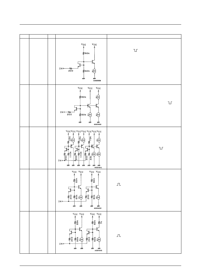
Equivalent circuit
37
38
39
40
41
C. CYNC
C. BLK
P. BLK
CLP2
CLP1
I
I
I
I
I
Composite synchronization signal pulse input. Sync is added to the
signal white clipped at pin 22 with the timing of the composite
synchronization pulse (
) signal input to this pin. Also, the signal
including synchronization is amplified by about 7.7 dB. When the pin
29 input signal level is set to 500 mV (white average), the signal
level, including setup and sync, is amplified to be 140 IRE = about
1.9 V when pin 31 is unloaded. Therefore the pin 31 output will be:
White average:
Saturation level:
= about 1220 mV
= about 1700 mV (when the pin 29 input
saturation level is about 700 mV)
= about 550 mV
Sync level:
Composite blanking pulse input. The signal OPB clamped at pin 24 is
blanked with the timing of the composite blanking pulse (
to this pin. Also, pedestal of the prescribed level is added with the
same timing and setup is also inserted. At that time, levels 250 mV or
more lower than the OPB level are low clipped.
) input
Pre-blanking pulse input. The other path for the signal that was
clipped by the post-CDS OPB goes to the iris amplifier system. First,
pedestal is added using the pre-blanking pulse (
pin. In addition, this signal is also used by the AGC detector system
and the
γ
correction system.
) input to this
Input for the output clamping pulse. This pin inputs the clamping
pulse (
) for OPB clamping used by pins 24, 25 and 29. The
clamping pulse timing is delayed with respect to CLP1 to take into
account the amount the signal is delayed within the IC and by the
external LPF. When 1H interpolation is used, the clamping pulse is
turned on or off every 1H with the timing of the LSP pulse. This is
then used as the OPB clamp for pins 24 and 25.
OPB clamp pulse input. The dark current variations every 1H are
taken up by clamping, with the OPB timing, the signal that became a
continuous wave signal in the CDS system. This pin is the clamp
pulse (
) input for that operation, and normally can be shared
with pin 42.
相關(guān)PDF資料 |
PDF描述 |
|---|---|
| LA7265 | Single-Chip Black and White CCD Camera signal Processing IC |
| LA72702VA | Monolithic Linear IC For US TV BTSC Decoder |
| LA7270 | VHS VTR Playback Head Amplifier Recording Amplifier |
| LA7270M | VHS VTR Playback Head Amplifier Recording Amplifier |
| LA72714VA | Monolithic Linear IC For JPN TV Multi Channel Television Sound Decoder IC |
相關(guān)代理商/技術(shù)參數(shù) |
參數(shù)描述 |
|---|---|
| LA7266M | 制造商:未知廠家 制造商全稱:未知廠家 功能描述: |
| LA72670BM | 制造商:SANYO 制造商全稱:Sanyo Semicon Device 功能描述:US multiplex modulation for VCR HiFi Sound Signal Processor |
| LA72670BM-MPB-E | 制造商:ON Semiconductor 功能描述: |
| LA72680M | 制造商:SANYO 制造商全稱:Sanyo Semicon Device 功能描述:JAPAN TV Sound Multiplex Demodulation HiFi Sound Signal Processor |
| LA72680M-MPB-E | 制造商:ON Semiconductor 功能描述: 制造商:Sony Semiconductor Solutions Division 功能描述: |
發(fā)布緊急采購,3分鐘左右您將得到回復。