- 您現(xiàn)在的位置:買賣IC網(wǎng) > PDF目錄373180 > KS9241B (SAMSUNG SEMICONDUCTOR CO. LTD.) CD-ROM Decoder(光盤驅(qū)動器解碼器) PDF資料下載
參數(shù)資料
| 型號: | KS9241B |
| 廠商: | SAMSUNG SEMICONDUCTOR CO. LTD. |
| 英文描述: | CD-ROM Decoder(光盤驅(qū)動器解碼器) |
| 中文描述: | 的CD - ROM解碼器(光盤驅(qū)動器解碼器) |
| 文件頁數(shù): | 25/37頁 |
| 文件大小: | 211K |
| 代理商: | KS9241B |
第1頁第2頁第3頁第4頁第5頁第6頁第7頁第8頁第9頁第10頁第11頁第12頁第13頁第14頁第15頁第16頁第17頁第18頁第19頁第20頁第21頁第22頁第23頁第24頁當(dāng)前第25頁第26頁第27頁第28頁第29頁第30頁第31頁第32頁第33頁第34頁第35頁第36頁第37頁
CD-ROM DECODER
KS9241B
25
If host reads data from FIFO when the first data is registered into FIFO, the output data will be invalid and in this
case, /DTOPR bit of ISTATE register will be
“
0
”
and /DREN pin will
“
L
”
only after reading is finished at host. Data
transmission is finished when host reads data so much as the byte number established by micom. The moment
host starts to read the last byte, /DTUOP bit of ISTATE register becomes
“
1
”
, and /DREN bit becomes
“
H
”
. While
host is reading the last byte, /DTE bit becomes
“
L
”
. During the period of finishing the reading to writing into
DTEACK register, /DTINT bit of ISTATE register becomes
“
0
”
. At this moment, if the DTIEN bit of ICONT is
“
1
”
the
/INT pin becomes
“
L
”
. /WAIT signal output occurs at /WAIT pin when /SEL pin is
“
H
”
. Besides, host starts to read
data from FIFO for data transmission then, and if no data is written in FIFO, the /WAIT pin becomes
“
L
”
. On
condition that /SEL pin is
“
L
”
, data demanding signal is generated at /WAIT pin. The /WAIT pin is valid only which
host is reading data. The signal waveform of the following picture explains the case of transmission of 4 byte from
1*st address.
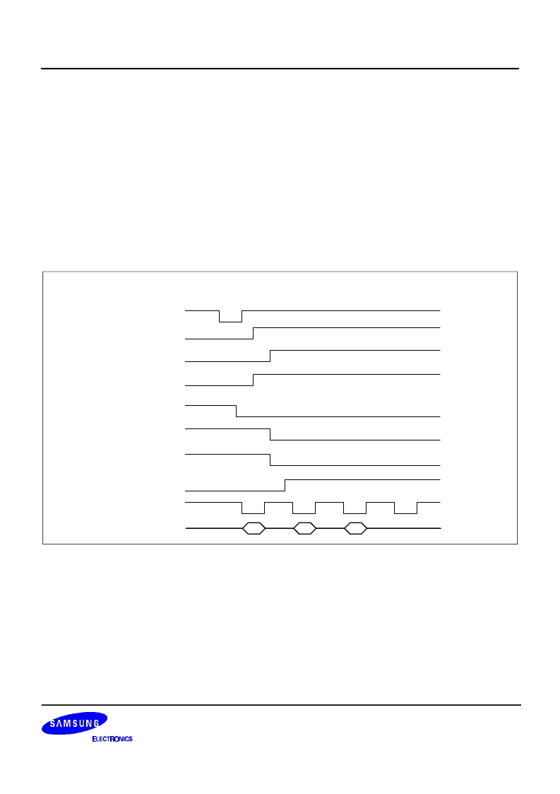
(ii) Wait Operation
(Wait Operation Timing)
Figure 19.
NOTE:
Condition : /HCS =
“
L
”
,/ CMD =
“
L
”
, /HWR =
“
L
”
/MCS =
“
L
”
, MRS =
“
H
”
, /MRD =
“
H
”
, Address Decoder =
“
0
”
If /DTWT bit of ICONT register is
“
0
”
, wait operation is started during status byte transmission. On condition that
the writing into DTSTR register is performed and finished by host, the /DTUOP bit of ISTATE register becomes
“
0
”
.
However, if status was then being transmitted, /DTOPR bit of ISTATE register becomes
“
0
”
and /DREN bit
becomes
“
L
”
, only when /STOPR bit of ISTATE register is
“
1
”
after status transmission is finished. After that, the
operation is as follows:
(Wait Operation Timming) /STWT =
“
0
”
)
(/DTWT =
“
0
”
) AD=6
/MWR
/STUOP
/STOPR
/SREN
/DTUOP
/DTOPR
/DREN
/CMD
/HRD
/HRD
/HD7-0.HDE
6
d1
d2
相關(guān)PDF資料 |
PDF描述 |
|---|---|
| KS9245 | Automated CD-ROM Controller(光盤驅(qū)動器控制器器) |
| KS9246 | ATAPI AUTOMATED CD-ROM CONTROLLER WITH EMBEDDED DRAM |
| KS9284 | Digital Signal Processor(數(shù)字信號處理器) |
| KSA1013 | PNP (COLOR TV AUDIO OUTPUT) |
| KSA1013 | Color TV Audio Output Color TV Vertical Deflection Output |
相關(guān)代理商/技術(shù)參數(shù) |
參數(shù)描述 |
|---|---|
| KS9246 | 制造商:SAMSUNG 制造商全稱:Samsung semiconductor 功能描述:ATAPI AUTOMATED CD-ROM CONTROLLER WITH EMBEDDED DRAM |
| KS926S2 | 制造商:FUJI 制造商全稱:Fuji Electric 功能描述:LOW LOSS SUPER HIGH SPEED RECTIFIER |
| KS926S2_07 | 制造商:FUJI 制造商全稱:Fuji Electric 功能描述:LOW LOSS SUPER HIGH SPEED RECTIFIER |
| KS9282B | 制造商:SAMSUNG 制造商全稱:Samsung semiconductor 功能描述:CMOS INTEGRATED CIRCUIT |
| KS9286 | 制造商:SAMSUNG 制造商全稱:Samsung semiconductor 功能描述:DIGITAL SIGNAL PROCESSOR for CDP |
發(fā)布緊急采購,3分鐘左右您將得到回復(fù)。