- 您現(xiàn)在的位置:買賣IC網(wǎng) > PDF目錄373155 > KM416RD16AD (SAMSUNG SEMICONDUCTOR CO. LTD.) CAP ELECT 47UF 100V TG SMD PDF資料下載
參數(shù)資料
| 型號: | KM416RD16AD |
| 廠商: | SAMSUNG SEMICONDUCTOR CO. LTD. |
| 英文描述: | CAP ELECT 47UF 100V TG SMD |
| 中文描述: | 128/144Mbit RDRAM的256 × 16/18位× 2 * 16屬銀行直接RDRAMTM |
| 文件頁數(shù): | 30/64頁 |
| 文件大?。?/td> | 4052K |
| 代理商: | KM416RD16AD |
第1頁第2頁第3頁第4頁第5頁第6頁第7頁第8頁第9頁第10頁第11頁第12頁第13頁第14頁第15頁第16頁第17頁第18頁第19頁第20頁第21頁第22頁第23頁第24頁第25頁第26頁第27頁第28頁第29頁當(dāng)前第30頁第31頁第32頁第33頁第34頁第35頁第36頁第37頁第38頁第39頁第40頁第41頁第42頁第43頁第44頁第45頁第46頁第47頁第48頁第49頁第50頁第51頁第52頁第53頁第54頁第55頁第56頁第57頁第58頁第59頁第60頁第61頁第62頁第63頁第64頁
Page 27
KM416RD8AC(D)/KM418RD8AC(D)
Direct RDRAM
Rev. 1.01 Oct. 1999
Control Register Packets
Table 14 summarizes the formats of the four packet types for
control register transactions. Table 15 summarizes the fields
that are used within the packets.
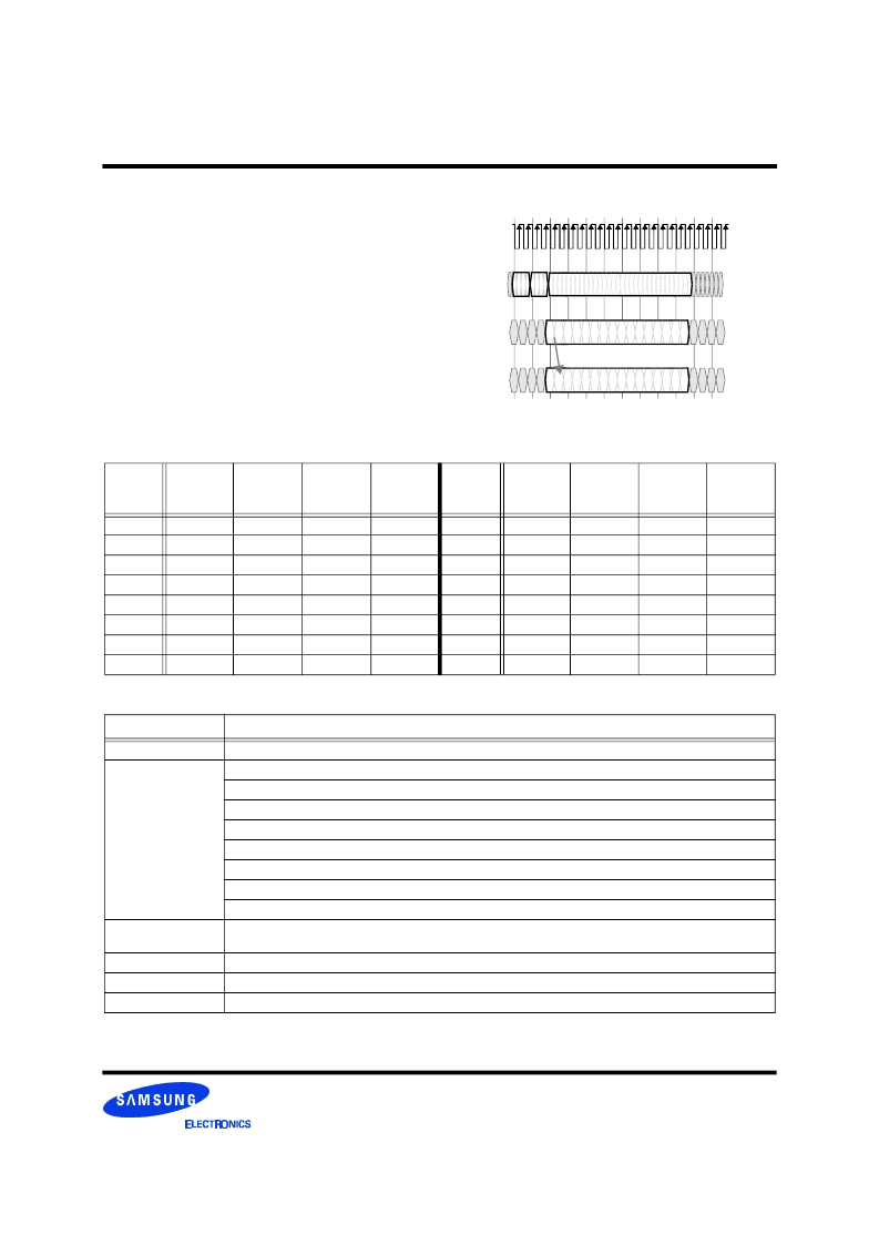
Figure 25 shows the transaction format for the SETR,
CLRR, and SETF commands. These transactions consist of a
single SRQ packet, rather than four packets like the SWR
and SRD commands. The same framing sequence on the
CMD input is used, however. These commands are used
during initialization prior to any control register read or
write transactions.
Figure 25: SETR, CLRR,SETF Transaction
SCK
CMD
SIO0
T
20
SRQ packet - SETR/CLRR/SETF
1111
00000000...00000000
SRQ packet - SETR/CLRR/SETF
0000
SIO1
T
4
The packet is repeated
from SIO0 to SIO1
1
1
1
1
0
0
0
0
Table 14: Control Register Packet Formats
SCK
Cycle
SIO0 or
SIO1
for SRQ
SIO0 or
SIO1
for SA
SIO0 or
SIO1
for SINT
SIO0 or
SIO1
for SD
SCK
Cycle
SIO0 or
SIO1
for SRQ
SIO0 or
SIO1
for SA
SIO0 or
SIO1
for SINT
SIO0 or
SIO1
for SD
0
rsrv
rsrv
0
SD15
8
SOP1
SA7
0
SD7
1
rsrv
rsrv
0
SD14
9
SOP0
SA6
0
SD6
2
rsrv
rsrv
0
SD13
10
SBC
SA5
0
SD5
3
rsrv
rsrv
0
SD12
11
SDEV4
SA4
0
SD4
4
rsrv
SA11
0
SD11
12
SDEV3
SA3
0
SD3
5
SDEV5
SA10
0
SD10
13
SDEV2
SA2
0
SD2
6
SOP3
SA9
0
SD9
14
SDEV1
SA1
0
SD1
7
SOP2
SA8
0
SD8
15
SDEV0
SA0
0
SD0
Table 15: Field Description for Control Register Packets
Field
Description
rsrv
Reserved. Should be driven as
“
0
”
by controller.
SOP3..SOP0
0000 - SRD. Serial read of control register {SA11..SA0} of RDRAM {SDEV5..SDEV0}.
0001 - SWR. Serial write of control register {SA11..SA0} of RDRAM {SDEV5..SDEV0}.
0010 - SETR. Set Reset bit, all control registers assume their reset values.
a
16 t
SCYCLE
delay until CLRR command.
0100 - SETF. Set fast (normal) clock mode. 4 t
SCYCLE
delay until next command.
1011 - CLRR. Clear Reset bit, all control registers retain their reset values.
a
4 t
SCYCLE
delay until next command.
1111 - NOP. No serial operation.
0011, 0101-1010, 1100-1110 - RSRV. Reserved encodings.
SDEV5..SDEV0
Serial device. Compared to SDEVID5..SDEVID0 field of INIT control register field to select the RDRAM to which the transac-
tion is directed.
SBC
Serial broadcast. When set, RDRAMs ignore {SDEV5..SDEV0} for RDRAM selection.
SA11..SA0
Serial address. Selects which control register of the selected RDRAM is read or written.
SD15..SD0
Serial data. The 16 bits of data written to or read from the selected control register of the selected RDRAM.
a. The SETR and CLRR commands must always be applied in two successive transactions to RDRAMs; i.e. they may not be used in isolation. This is called
“
SETR/CLRR Reset
”
.
相關(guān)PDF資料 |
PDF描述 |
|---|---|
| KM416RD16C | 15VPP 74DB 2 TERM CERAM BUZZER |
| KM416RD16D | 15VPP 86DB 2 TERM CERAM BUZZER |
| KM416RD2AC | 128/144Mbit RDRAM 256K x 16/18 bit x 2*16 Dependent Banks Direct RDRAMTM |
| KM416RD2AD | 128/144Mbit RDRAM 256K x 16/18 bit x 2*16 Dependent Banks Direct RDRAMTM |
| KM416RD2C | 128/144Mbit RDRAM 256K x 16/18 bit x 2*16 Dependent Banks Direct RDRAMTM |
相關(guān)代理商/技術(shù)參數(shù) |
參數(shù)描述 |
|---|---|
| KM416RD16C | 制造商:SAMSUNG 制造商全稱:Samsung semiconductor 功能描述:128/144Mbit RDRAM 256K x 16/18 bit x 2*16 Dependent Banks Direct RDRAMTM |
| KM416RD16D | 制造商:SAMSUNG 制造商全稱:Samsung semiconductor 功能描述:128/144Mbit RDRAM 256K x 16/18 bit x 2*16 Dependent Banks Direct RDRAMTM |
| KM416RD2AC | 制造商:SAMSUNG 制造商全稱:Samsung semiconductor 功能描述:128/144Mbit RDRAM 256K x 16/18 bit x 2*16 Dependent Banks Direct RDRAMTM |
| KM416RD2AD | 制造商:SAMSUNG 制造商全稱:Samsung semiconductor 功能描述:128/144Mbit RDRAM 256K x 16/18 bit x 2*16 Dependent Banks Direct RDRAMTM |
| KM416RD2C | 制造商:SAMSUNG 制造商全稱:Samsung semiconductor 功能描述:128/144Mbit RDRAM 256K x 16/18 bit x 2*16 Dependent Banks Direct RDRAMTM |
發(fā)布緊急采購,3分鐘左右您將得到回復(fù)。