- 您現(xiàn)在的位置:買賣IC網(wǎng) > PDF目錄374353 > KM29V64000T (SAMSUNG SEMICONDUCTOR CO. LTD.) 8M x 8 Bit NAND Flash Memory(8M x 8位 NAND閃速存儲器) PDF資料下載
參數(shù)資料
| 型號: | KM29V64000T |
| 廠商: | SAMSUNG SEMICONDUCTOR CO. LTD. |
| 英文描述: | 8M x 8 Bit NAND Flash Memory(8M x 8位 NAND閃速存儲器) |
| 中文描述: | 8米× 8位NAND閃存(8米× 8位的NAND閃速存儲器) |
| 文件頁數(shù): | 18/24頁 |
| 文件大小: | 293K |
| 代理商: | KM29V64000T |
KM29V64000T
FLASH MEMORY
18
DEVICE OPERATION
PAGE READ
Upon initial device power up, the device defaults to Read1 mode. This operation is also initiated by writing 00H to the command reg-
ister along with three address cycles. Once the command is latched, it does not need to be written for the following page read o per-
ation. Three types of operations are available : random read, serial page read and sequential row read.
The random read mode is enabled when the page address is changed. The 528 bytes of data within the selected page are trans-
ferred to the data registers in less than 7
μ
s(tR). The CPU can detect the completion of this data transfer(tR) by analyzing the output
of R/B pin. Once the data in a page is loaded into the registers, they may be read out in 50ns cycle time by sequentially pulsing RE.
High to low transitions of the RE clock output the data stating from the selected column address up to the last column address(col-
umn 511 or 527 depending on the state of SE pin).
After the data of last column address is clocked out, the next page is automatically selected for sequential row read.
Waiting 7
μ
s again allows reading the selected page.The sequential row read operation is terminated by bringing CE high. The way
the Read1 and Read2 commands work is like a pointer set to either the main area or the spare area. The spare area of bytes 512 t o
527 may be selectively accessed by writing the Read2 command with SE pin low. Addresses A
0
to A
3
set the starting address of the
spare area while addresses A
4
to A
7
are ignored. Unless the operation is aborted, the page address is automatically incremented for
sequential row read as in Read1 operation and spare sixteen bytes of each page may be sequentially read. The Read1 com-
mand(00H/01H) is needed to move the pointer back to the main area. Figures 3 thru 6 show typical sequence and timings for each
read operation.
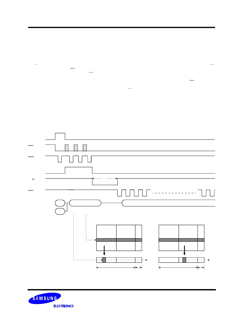
Figure 3. Read1 Operation
Start Add.(3Cycle)
00H
01H
A
0
~ A
7
& A
9
~ A
22
Data Output(Sequential)
(00H Command)
1st half array 2nd half array
Data Field
Spare Field
(01H Command)*
1st half array 2nd half array
Data Field
Spare Field
* After data access on 2nd half array by 01H command, the start pointer is automatically moved to 1st half array (00H) at next cycle.
CE
CLE
ALE
R/B
WE
I/O
0
~
7
RE
t
R
相關(guān)PDF資料 |
PDF描述 |
|---|---|
| KM29V64001RS | 8M X 8 BIT NAND FLASH MEMORY |
| KM29V64001TS | 8M X 8 BIT NAND FLASH MEMORY |
| KM29V64001T | 8M X 8 BIT NAND FLASH MEMORY |
| KM29W040AIT | 512K x 8 Bit NAND Flash Memory(512K x 8位 NAND閃速存儲器) |
| KM29W16000AIT | 2M x 8 Bit NAND Flash Memory(2M x 8位 NAND閃速存儲器) |
相關(guān)代理商/技術(shù)參數(shù) |
參數(shù)描述 |
|---|---|
| KM29V64000TS | 制造商:SAMSUNG 制造商全稱:Samsung semiconductor 功能描述:8M X 8 BIT NAND FLSH MEMORY |
| KM29V64001RS | 制造商:SAMSUNG 制造商全稱:Samsung semiconductor 功能描述:8M X 8 BIT NAND FLASH MEMORY |
| KM29V64001T | 制造商:SAMSUNG 制造商全稱:Samsung semiconductor 功能描述:8M X 8 BIT NAND FLASH MEMORY |
| KM29V64001TS | 制造商:SAMSUNG 制造商全稱:Samsung semiconductor 功能描述:8M X 8 BIT NAND FLASH MEMORY |
| KM29W040AT | 制造商:SAMSUNG 制造商全稱:Samsung semiconductor 功能描述:512K x 8 bit NAND Flash Memory |
發(fā)布緊急采購,3分鐘左右您將得到回復(fù)。