- 您現(xiàn)在的位置:買賣IC網(wǎng) > PDF目錄373124 > KFG1216D2A-FIB5 (SAMSUNG SEMICONDUCTOR CO. LTD.) FLASH MEMORY PDF資料下載
參數(shù)資料
| 型號: | KFG1216D2A-FIB5 |
| 廠商: | SAMSUNG SEMICONDUCTOR CO. LTD. |
| 英文描述: | FLASH MEMORY |
| 中文描述: | 閃存 |
| 文件頁數(shù): | 90/114頁 |
| 文件大小: | 1382K |
| 代理商: | KFG1216D2A-FIB5 |
第1頁第2頁第3頁第4頁第5頁第6頁第7頁第8頁第9頁第10頁第11頁第12頁第13頁第14頁第15頁第16頁第17頁第18頁第19頁第20頁第21頁第22頁第23頁第24頁第25頁第26頁第27頁第28頁第29頁第30頁第31頁第32頁第33頁第34頁第35頁第36頁第37頁第38頁第39頁第40頁第41頁第42頁第43頁第44頁第45頁第46頁第47頁第48頁第49頁第50頁第51頁第52頁第53頁第54頁第55頁第56頁第57頁第58頁第59頁第60頁第61頁第62頁第63頁第64頁第65頁第66頁第67頁第68頁第69頁第70頁第71頁第72頁第73頁第74頁第75頁第76頁第77頁第78頁第79頁第80頁第81頁第82頁第83頁第84頁第85頁第86頁第87頁第88頁第89頁當(dāng)前第90頁第91頁第92頁第93頁第94頁第95頁第96頁第97頁第98頁第99頁第100頁第101頁第102頁第103頁第104頁第105頁第106頁第107頁第108頁第109頁第110頁第111頁第112頁第113頁第114頁
OneNAND512(KFG1216x2A-xxB5)
FLASH MEMORY
90
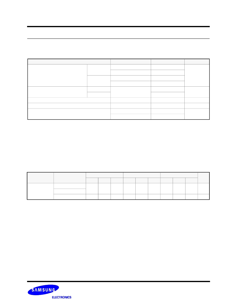
4.1 Absolute Maximum Ratings
NOTES
:
1. Minimum DC voltage is -0.5V on Input/ Output pins. During transitions, this level should not fall to POR level(typ. 1.5V@1.8V device, 1.8V@2.65V/
3.3V device). Maximum DC voltage is Vcc+0.6V on input / output pins which, during transitions, may overshoot to Vcc+2.0V for periods <20ns.
2. Permanent device damage may occur if ABSOLUTE MAXIMUM RATINGS are exceeded. Functional operation should be restricted to the conditions
detailed in the operational sections of this data sheet. Exposure to absolute maximum rating conditions for extended periods may affect reliability.
Parameter
Symbol
Rating
Unit
Voltage on any pin relative to V
SS
Vcc
Vcc (for 1.8V)
-0.5 to + 2.45
V
Vcc (for 2.65V/3.3V)
-0.5 to + 4.6
All Pins
V
IN
(for 1.8V)
V
IN
(for 2.65V/3.3V)
-0.5 to + 2.45
-0.5 to + 4.6
Temperature Under Bias
Extended
T
bias
-30 to +125
°
C
Industrial
-40 to +125
Storage Temperature
T
stg
-65 to +150
°
C
Short Circuit Output Current
I
OS
5
mA
Recommended Operating Temperature
T
A
(Extended Temp.)
-30 to +85
°
C
T
A
(Industrial Temp.)
-40 to +85
4.2 Operating Conditions
4.0 DC CHARACTERISTICS
Voltage reference to GND
NOTES
:
1. The system power should reach 1.7V after POR triggering level(typ. 1.5V) within 400us.
For 2.65V and 3.3V device, the system power should reach 2.2V after POR triggering level(typ. 1.8V) within 400us.
2. Vcc-Core (or Vcc) should reach the operating voltage level prior to or at the same time as Vcc-IO (or Vccq).
Parameter
Symbol
1.8V Device
2.65V Device
3.3V Device
Unit
Min
Typ.
Max
Min
Typ.
Max
Min
Typ.
Max
Supply Voltage
V
CC-
core / Vcc
1.7
1.8
1.95
2.4
2.65
2.9
2.7
3.3
3.6
V
V
CC-
IO / Vccq
V
SS
0
0
0
0
0
0
0
0
0
V
相關(guān)PDF資料 |
PDF描述 |
|---|---|
| KFG1216D2A-FIB6 | FLASH MEMORY |
| KFG1216D2A-FID5 | FLASH MEMORY |
| KFG1216D2A-FID6 | FLASH MEMORY |
| KFG1216Q2A-DEB5 | FLASH MEMORY |
| KFG1216Q2A-DEB6 | FLASH MEMORY |
相關(guān)代理商/技術(shù)參數(shù) |
參數(shù)描述 |
|---|---|
| KFG1216D2A-FIB6 | 制造商:SAMSUNG 制造商全稱:Samsung semiconductor 功能描述:FLASH MEMORY |
| KFG1216D2A-FID5 | 制造商:SAMSUNG 制造商全稱:Samsung semiconductor 功能描述:FLASH MEMORY |
| KFG1216D2A-FID6 | 制造商:SAMSUNG 制造商全稱:Samsung semiconductor 功能描述:FLASH MEMORY |
| KFG1216D2M-DEB | 制造商:SAMSUNG 制造商全稱:Samsung semiconductor 功能描述:FLASH MEMORY |
| KFG1216D2M-DED | 制造商:SAMSUNG 制造商全稱:Samsung semiconductor 功能描述:FLASH MEMORY |
發(fā)布緊急采購,3分鐘左右您將得到回復(fù)。