- 您現(xiàn)在的位置:買(mǎi)賣(mài)IC網(wǎng) > PDF目錄373088 > K9F6408U0C-T (SAMSUNG SEMICONDUCTOR CO. LTD.) 8M x 8 Bit NAND Flash Memory PDF資料下載
參數(shù)資料
| 型號(hào): | K9F6408U0C-T |
| 廠商: | SAMSUNG SEMICONDUCTOR CO. LTD. |
| 英文描述: | 8M x 8 Bit NAND Flash Memory |
| 中文描述: | 8米× 8位NAND閃存 |
| 文件頁(yè)數(shù): | 27/30頁(yè) |
| 文件大小: | 784K |
| 代理商: | K9F6408U0C-T |
第1頁(yè)第2頁(yè)第3頁(yè)第4頁(yè)第5頁(yè)第6頁(yè)第7頁(yè)第8頁(yè)第9頁(yè)第10頁(yè)第11頁(yè)第12頁(yè)第13頁(yè)第14頁(yè)第15頁(yè)第16頁(yè)第17頁(yè)第18頁(yè)第19頁(yè)第20頁(yè)第21頁(yè)第22頁(yè)第23頁(yè)第24頁(yè)第25頁(yè)第26頁(yè)當(dāng)前第27頁(yè)第28頁(yè)第29頁(yè)第30頁(yè)
FLASH MEMORY
27
K9F6408U0C
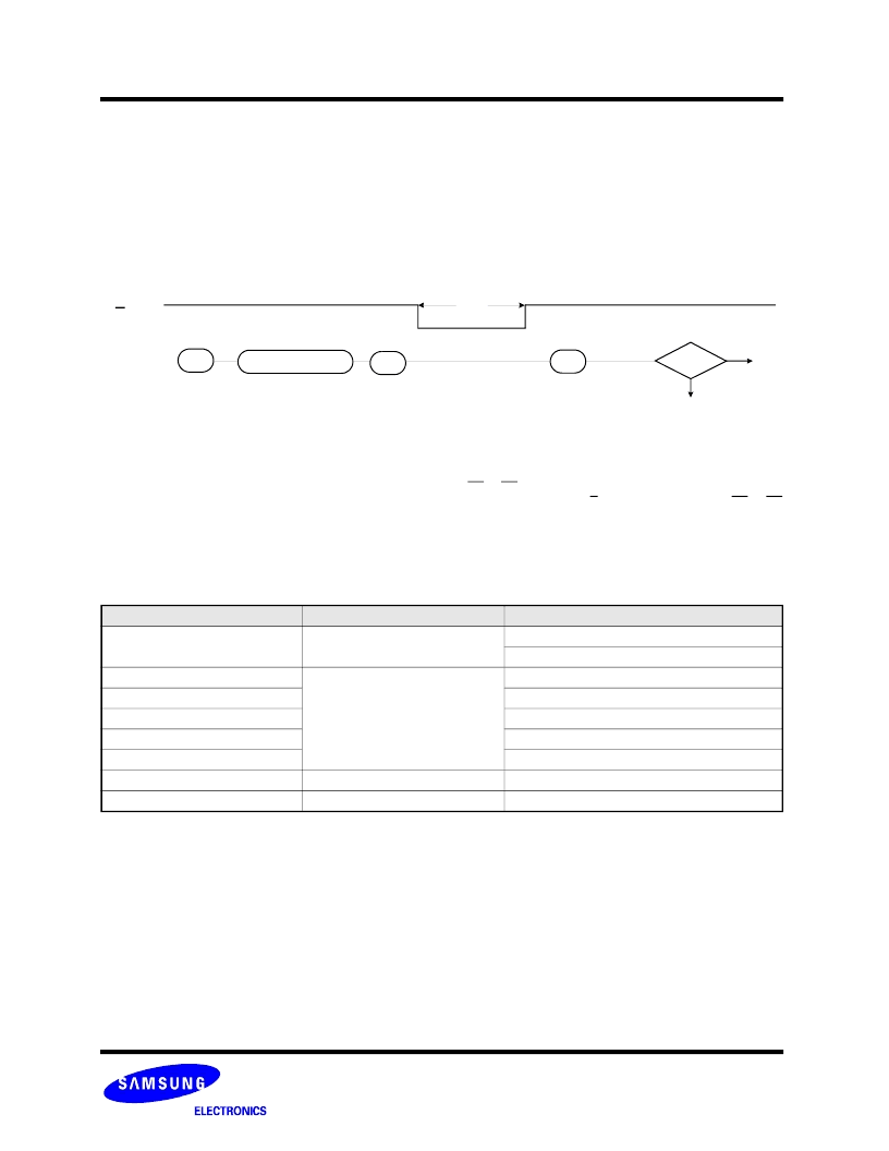
Figure 8. Block Erase Operation
BLOCK ERASE
The Erase operation is done on a block(8K Byte) basis. Block address loading is accomplished in two cycles initiated by an Erase
Setup command(60h). Only address A
13
to A
22
is valid while A
9
to A
12
is ignored. The Erase Confirm command(D0h) following the
block address loading initiates the internal erasing process. This two-step sequence of setup followed by execution command
ensures that memory contents are not accidentally erased due to external noise conditions.
At the rising edge of WE after the erase confirm command input, the internal write controller handles erase and erase-verify. When
the erase operation is completed, the Write Status Bit(I/O 0) may be checked.
Figure 8 details the sequence.
60h
Block Add. : A
9
~ A
22
I/O
0
~
7
R/B
Address Input(2Cycle)
I/O
0
Pass
D0h
70h
Fail
t
BERS
READ STATUS
The device contains a Status Register which may be read to find out whether program or erase operation is completed, and whether
the program or erase operation is completed successfully. After writing 70h command to the command register, a read cycle outputs
the content of the Status Register to the I/O pins on the falling edge of CE or RE, whichever occurs last. This two line control allows
the system to poll the progress of each device in multiple memory connections even when R/B pins are common-wired. RE or CE
does not need to be toggled for updated status. Refer to table 2 for specific Status Register definitions. The command register
remains in Status Read mode until further commands are issued to it. Therefore, if the status register is read during a random read
cycle, a read command(00h or 50h) should be given before sequential page read cycle.
Table2. Read Status Register Definition
I/O #
Status
Definition
I/O
0
Program / Erase
"0" : Successful Program / Erase
"1" : Error in Program / Erase
I/O
1
Reserved for Future
Use
"0"
I/O
2
"0"
I/O
3
"0"
I/O
4
"0"
I/O
5
"0"
I/O
6
Device Operation
"0" : Busy "1" : Ready
I/O
7
Write Protect
"0" : Protected "1" : Not Protected
相關(guān)PDF資料 |
PDF描述 |
|---|---|
| K9F6408U0C-V | 8M x 8 Bit NAND Flash Memory |
| K9F6408U0C | 8M x 8 Bit NAND Flash Memory |
| K9K1208D0C | TV 37C 37#16 SKT RECP |
| K9K1216Q0C | SCSI 2 MALE-MALE 3 FT |
| K9K1216U0C | M1 - DVI-D W/USB 10 FEET |
相關(guān)代理商/技術(shù)參數(shù) |
參數(shù)描述 |
|---|---|
| K9F6408U0C-V | 制造商:SAMSUNG 制造商全稱:Samsung semiconductor 功能描述:8M x 8 Bit NAND Flash Memory |
| K9F6408U0M-TCB0 | 制造商:SAMSUNG 制造商全稱:Samsung semiconductor 功能描述:8M x 8 Bit NAND Flash Memory |
| K9F6408U0M-TIB0 | 制造商:SAMSUNG 制造商全稱:Samsung semiconductor 功能描述:8M x 8 Bit NAND Flash Memory |
| K9F8008W0M- | 制造商:SAMSUNG 制造商全稱:Samsung semiconductor 功能描述:1M x 8 bit NAND Flash Memory |
| K9F8008W0M-TCB0 | 制造商:SAMSUNG 制造商全稱:Samsung semiconductor 功能描述:1M x 8 bit NAND Flash Memory |
發(fā)布緊急采購(gòu),3分鐘左右您將得到回復(fù)。