- 您現(xiàn)在的位置:買賣IC網(wǎng) > PDF目錄374296 > K9F1608W0A-TCB0 (SAMSUNG SEMICONDUCTOR CO. LTD.) TV 128C 128#22D SKT RECP PDF資料下載
參數(shù)資料
| 型號: | K9F1608W0A-TCB0 |
| 廠商: | SAMSUNG SEMICONDUCTOR CO. LTD. |
| 英文描述: | TV 128C 128#22D SKT RECP |
| 中文描述: | 200萬× 8位NAND閃存 |
| 文件頁數(shù): | 6/25頁 |
| 文件大?。?/td> | 443K |
| 代理商: | K9F1608W0A-TCB0 |
K9F1608W0A-TCB0, K9F1608W0A-TIB0
FLASH MEMORY
6
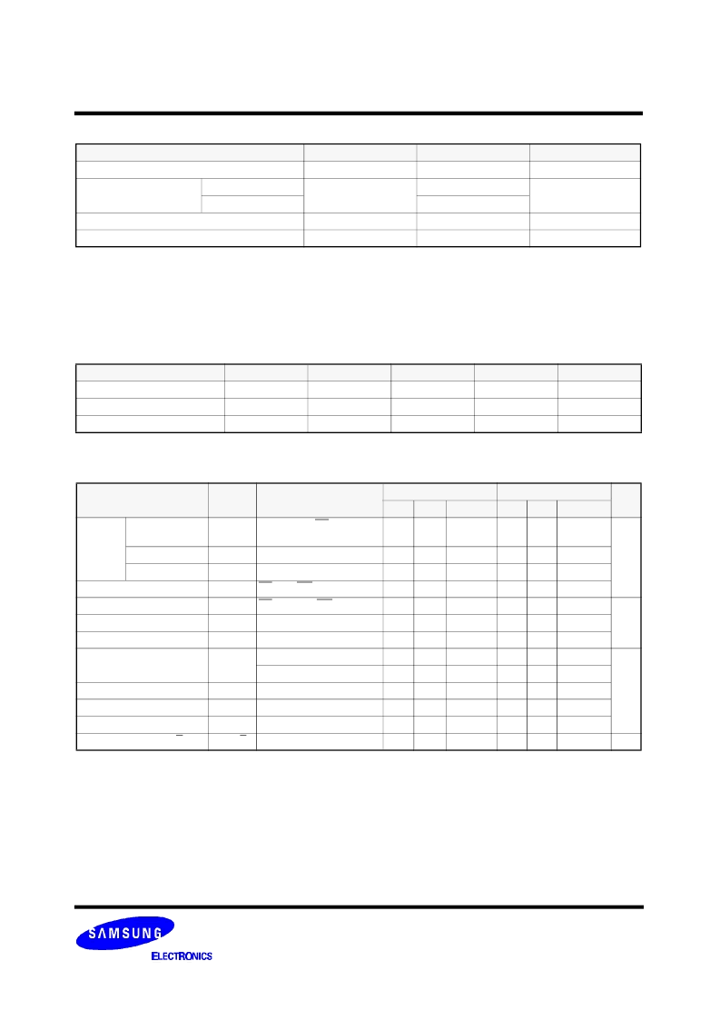
DC AND OPERATING CHARACTERISTICS
(Recommended operating conditions otherwise noted.)
Parameter
Symbol
Test Conditions
Vcc=2.7V ~ 3.6V
Vcc=3.6V ~ 5.5V
Unit
Min
Typ
Max
Min
Typ
Max
Operating
Current
Sequential Read
I
CC
1
tcycle=80ns, CE=V
IL
,
I
OUT
=0mA
-
10
20
-
15
30
mA
Program
I
CC
2
-
-
10
20
-
15
30
Erase
I
CC
3
-
-
10
20
-
25
40
Stand-by Current(TTL)
I
SB
1
CE=V
IH
, WP=0V/V
CC
-
-
1
-
-
1
Stand-by Current(CMOS)
I
SB
2
CE=V
CC
-0.2, WP=0V/V
CC
-
5
50
-
5
50
μ
A
Input Leakage Current
I
LI
V
IN
=0 to 5.5V
-
-
±
10
±
10
-
-
±
10
±
10
Output Leakage Current
I
LO
V
OUT
=0 to 5.5V
-
-
-
-
Input High Voltage
V
IH
I/O Pins
2.0
-
V
CC
Q+0.3
3.0
-
V
CC
Q+0.5
V
Except I/O Pins
2.0
-
V
CC
+0.3
3.0
-
V
CC
+0.5
Input Low Voltage, All inputs
V
IL
-
-0.3
-
0.6
-0.3
-
0.8
Output High Voltage Level
V
OH
I
OH
=-400
μ
A
2.4
-
-
2.4
-
-
Output Low Voltage Level
V
OL
I
OL
=2.1mA
-
-
0.4
-
-
0.4
Output Low Current(R/B)
I
OL
(R/B)
V
OL
=0.4V
8
10
-
8
10
-
mA
ABSOLUTE MAXIMUM RATINGS
NOTE
:
1. Minimum DC voltage is -0.3V on input/output pins. During transitions, this level may undershoot to -2.0V for periods <30ns.
Maximum DC voltage on input/output pins is V
CC
Q+0.3V which, during transitions, may overshoot to V
CC
+2.0V for periods <20ns.
2. Permanent device damage may occur if ABSOLUTE MAXIMUM RATINGS are exceeded. Functional operation should be restricted to the conditions
as detailed in the operational sections of this data sheet. Exposure to absolute maximum rating conditions for extended periods may affect reliability.
Parameter
Symbol
Rating
Unit
Voltage on any pin relative to V
SS
V
IN
-0.6 to +7.0
V
Temperature Under Bias
K9F1608W0A-TCB0
T
BIAS
-10 to +125
°
C
K9F1608W0A-TIB0
-40 to +125
Storage Temperature
T
STG
-65 to +150
°
C
Short Circuit Output Current
I
OS
5
mA
RECOMMENDED OPERATING CONDITIONS
(Voltage reference to GND, K9F1608W0A-TCB0
:
T
A
=0 to 70
°
C, K9F1608W0A-TIB0
:
T
A
=-40 to 85
°
C)
NOTE
: 1. Vcc and VccQ pins are separater each other.
Parameter
Symbol
Min
Typ.
Max
Unit
Supply Voltage
V
CC
2.7
-
5.5
V
Supply Voltage
V
CC
Q
1)
V
SS
2.7
-
5.5
V
Supply Voltage
0
0
0
V
相關(guān)PDF資料 |
PDF描述 |
|---|---|
| K9F1608W0A-TIB0 | TV 37C 37#16 PIN RECP |
| K9F1G08Q0A | FLASH MEMORY |
| K9F1G08U0A | FLASH MEMORY |
| K9F1G08Q0M-YIB0 | 1Gb Gb 1.8V NAND Flash Errata |
| K9F1G16Q0M-YCB0 | 1Gb Gb 1.8V NAND Flash Errata |
相關(guān)代理商/技術(shù)參數(shù) |
參數(shù)描述 |
|---|---|
| K9F1608W0A-TIB0 | 制造商:SAMSUNG 制造商全稱:Samsung semiconductor 功能描述:2M x 8 Bit NAND Flash Memory |
| K9F1G08B0C-PCB0T00 | 制造商:Samsung Semiconductor 功能描述:1GB SLC NORMAL X8 FBGA - Trays |
| K9F1G08D0M | 制造商:SAMSUNG 制造商全稱:Samsung semiconductor 功能描述:128M x 8 Bit / 64M x 16 Bit NAND Flash Memory |
| K9F1G08Q0A | 制造商:SAMSUNG 制造商全稱:Samsung semiconductor 功能描述:FLASH MEMORY |
| K9F1G08Q0M | 制造商:SAMSUNG 制造商全稱:Samsung semiconductor 功能描述:128M x 8 Bit / 64M x 16 Bit NAND Flash Memory |
發(fā)布緊急采購,3分鐘左右您將得到回復(fù)。