- 您現(xiàn)在的位置:買賣IC網(wǎng) > PDF目錄374277 > K4R271669E (SAMSUNG SEMICONDUCTOR CO. LTD.) 128Mbit RDRAM(E-die) PDF資料下載
參數(shù)資料
| 型號: | K4R271669E |
| 廠商: | SAMSUNG SEMICONDUCTOR CO. LTD. |
| 英文描述: | 128Mbit RDRAM(E-die) |
| 中文描述: | 128Mbit的RDRAM(電子模具) |
| 文件頁數(shù): | 17/20頁 |
| 文件大小: | 290K |
| 代理商: | K4R271669E |
Page 15
Direct RDRAM
K4R271669E
Version 1.4 July 2002
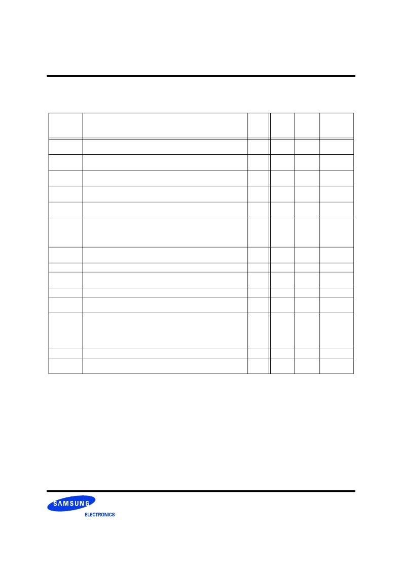
Timing Parameters
Table 13: Timing Parameter Summary
Parameter
Description
Min
-45
-800
Max
Units
Figure(s)
t
RC
Row Cycle time of RDRAM banks -the interval between ROWA packets with ACT
commands to the same bank.
28
-
t
CYCLE
Figure 16
Figure 17
t
RAS
RAS-asserted time of RDRAM bank - the interval between ROWA packet with
ACT command and next ROWR packet with PRER
a
command to the same bank.
20
64
μ
s
b
t
CYCLE
Figure 16
Figure 17
t
RP
Row Precharge time of RDRAM banks - the interval between ROWR packet with
PRER
a
command and next ROWA packet with ACT command to the same bank.
8
-
t
CYCLE
Figure 16
Figure 17
t
PP
Precharge-to-precharge time of RDRAM device - the interval between successive
ROWR packets with PRER
a
commands to any banks of the same device.
8
-
t
CYCLE
Figure 13
t
RR
RAS-to-RAS time of RDRAM device - the interval between successive ROWA
packets with ACT commands to any banks of the same device.
8
-
t
CYCLE
Figure 14
t
RCD
RAS-to-CAS Delay - the interval from ROWA packet with ACT command to
COLC packet with RD or WR command). Note - the RAS-to-CAS delay seen by
the RDRAM core (t
RCD-C
) is equal to t
RCD-C
= 1 + t
RCD
because of differences in
the row and column paths through the RDRAM interface.
9
-
t
CYCLE
Figure 16
Figure 17
t
CAC
CAS Access delay - the interval from RD command to Q read data. The equation
for t
CAC
is given in the TPARM register in Figure 40.
8
12
t
CYCLE
Figure 5
Figure 40
t
CWD
CAS Write Delay (interval from WR command to D write data.
6
6
t
CYCLE
Figure 5
t
CC
CAS-to-CAS time of RDRAM bank - the interval between successive COLC com-
mands).
4
-
t
CYCLE
Figure 16
Figure 17
t
PACKET
Length of ROWA, ROWR, COLC, COLM or COLX packet.
4
4
t
CYCLE
Figure 3
t
RTR
Interval from COLC packet with WR command to COLC packet which causes
retire, and to COLM packet with bytemask.
8
-
t
CYCLE
Figure 18
t
OFFP
The interval (offset) from COLC packet with RDA command, or from COLC
packet with retire command (after WRA automatic precharge), or from COLC
packet with PREC command, or from COLX packet with PREX command to the
equivalent ROWR packet with PRER. The equation for t
OFFP
is given in the
TPARM register in Figure 40.
4
4
t
CYCLE
Figure 15
Figure 40
t
RDP
Interval from last COLC packet with RD command to ROWR packet with PRER.
4
-
t
CYCLE
Figure 16
t
RTP
Interval from last COLC packet with automatic retire command to ROWR packet
with PRER.
4
-
t
CYCLE
Figure 17
a. Or equivalent PREC or PREX command. See Figure 15.
b. This is a constraint imposed by the core, and is therefore in units of
μ
s rather than t
CYCLE
.
相關(guān)PDF資料 |
PDF描述 |
|---|---|
| K4R571669D | 256/288Mbit RDRAM(D-die) |
| K4R881869D | 256/288Mbit RDRAM(D-die) |
| K4R761869A-GCN1 | 576Mbit RDRAM (A-die) 1M x 18bit x 32s banks Direct RDRAMTM |
| K4R761869A-GCT9 | 576Mbit RDRAM (A-die) 1M x 18bit x 32s banks Direct RDRAMTM |
| K4R761869A-F | 576Mbit RDRAM (A-die) 1M x 18bit x 32s banks Direct RDRAMTM |
相關(guān)代理商/技術(shù)參數(shù) |
參數(shù)描述 |
|---|---|
| K4R271669F | 制造商:SAMSUNG 制造商全稱:Samsung semiconductor 功能描述:128Mbit RDRAM(F-die) |
| K4R271669F-RCS8000 | 制造商:Samsung 功能描述:128 DIRECT RDRAM X16 WBGA - Trays |
| K4R271669F-TCS8000 | 制造商:Samsung 功能描述:128 DIRECT RDRAM X16 WBGA - Trays |
| K4R271669H-DCS8000 | 制造商:Samsung Semiconductor 功能描述:128MRDRAMDIRECT RDRAMX16FBGA - Bulk |
| K4R271669H-DCS8T00 | 制造商:Samsung Semiconductor 功能描述:128MRDRAMDIRECT RDRAMX16FBGA - Tape and Reel |
發(fā)布緊急采購,3分鐘左右您將得到回復(fù)。