- 您現(xiàn)在的位置:買賣IC網(wǎng) > PDF目錄383186 > IXBD4410SI (IXYS CORP) MICA RoHS Compliant: No PDF資料下載
參數(shù)資料
| 型號: | IXBD4410SI |
| 廠商: | IXYS CORP |
| 元件分類: | MOSFETs |
| 英文描述: | MICA RoHS Compliant: No |
| 中文描述: | 2 A HALF BRDG BASED MOSFET DRIVER, PDSO16 |
| 封裝: | PLASTIC, SOIC-16 |
| 文件頁數(shù): | 10/11頁 |
| 文件大?。?/td> | 705K |
| 代理商: | IXBD4410SI |
2004 IXYS All rights reserved
IXBD4410
IXBD4411
If the MOSFET switched 25 A, the
transient will last as long as (25/500)
μ
s
or 50 ns, which is more than the typical
6 or 7 ns propagations or of a 74HC
series gate.
conversion equipment due to their very
high common mode dv/dt rejection
capabilities.
Transformer Considerations
The transformer is the communication
link and isolation barrier between the
high- and low-side ICs. The high-side
gate and fault signals are transmitted
through the transformer while main-
taining the proper isolation. The
transmitter signal is in the form of a
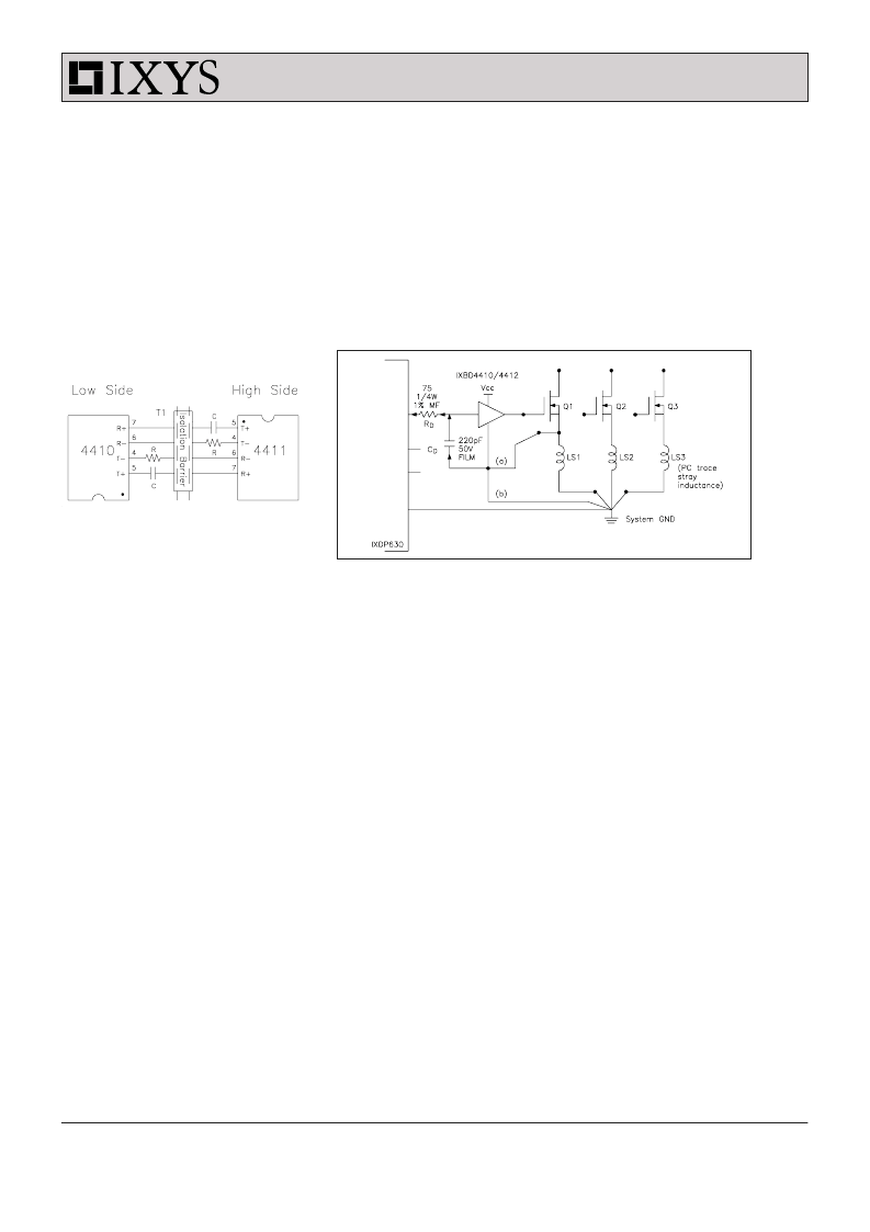
Fig. 10: Potential layout problems that create functional problems
MOSFET on, continuing the oscillation
for one more cycle.
To eliminate this problem, a ground
level transformation circuit must be
added, that rejects this common mode
transient. The simplest is a de-coupling
circuit, also illustrated in Fig. 10. The
capacitor voltage on C
remains
constant while the transient voltage is
dropped across R
and the driver
detects no input transition, eliminating
the oscillation. This circuit does add
significantly to turn-on and turn-off delay
time, and cannot be used if the transient
lasts longer than the allowable delays.
Delay times must be considered in
selection of system dead time.
The most complex (and most effective)
method of eliminating the effects of
transients between grounds is isolation.
Optocouplers and pulse transformers
are the most commonly used isolation
techniques, and work very well in this
case. The IXDP630/631 has been
specifically designed to directly drive a
high speed optocoupler like the Hewlett
Packard HCPL22XX family or the
General Instrument 740L60XX optologic
family. These optos are especially well
suited to motor control and power
square wave, but the receiver responds
only to the logic edges. This allows for
much smaller transformer designs,
since a 10 kHz switching frequency
does not require a 10 kHz pulse
transformer.
The recommended transformer for this
ISOSMART driver chipset is
fabricated using a very small ferrite
shield bead (see Fig. 11), onto which a
six-turn primary and a two-turn
secondary winding of 36 AWG magnet
wire are made. The two windings are
segment wound to achieve primary-to-
secondary isolation of up to 2500 V~.
The six-turn primaries are connected to
the respective IXBD4410/4411
transmitter outputs and the two-turn
secondaries are connected to their
respective receiver inputs.
Fig. 9: Suggested IC Orientation
Fig. 10 illustrates an example layout
problem. The power circuit consists of
three power transistors (MOSFETs in
this example). With the ISOSMART
gate driver chipset grounded as in
option (b) in Fig. 10, the communication
path from the IXDP630 will operate
without errors. The PC trace induced
voltages are not common with the digital
path, so the input of the gate driver will
not see or respond to them.
Unfortunately, the MOSFET will not
operate properly. The voltage induced
across LS1 when Q1 is turned on, acts
as source degeneration, modifying the
turn-on behavior of the MOSFET. If
LS1= 27 nH, and V
is 15 V (assuming
the gate plateau of the MOSFET
is 6
V),
the di/dt at turn-on will be regulated by
the driver/MOSFET/LS1 loop to about
200 A/
μ
s; quite a surprise when your
circuit requires 500 A/
μ
s to operate
correctly.
It is possible to make use of this
behavior to create a turn-on or turn-off
di/dt limiter (perhaps to snub the upper
free wheeling diode reverse recovery).
While possible, this is normally not
desirable or practical where two or more
transistors are controlled. Equalizing the
parasitic impedances of three traces
while positioning the transistors next to
their heat sink and meeting UL/VDE
voltage spacings is just too difficult.
Grounding the gate driver as in option
(a) in Fig. 10 solves the MOSFET turn
on problem by eliminating LS1 from the
source feedback loop. Now, unfor-
tunately, the gate driver will oscillate
every time it is turned on or off. As the
IXDP630 output goes "high", the gate
drive output follows (after its propaga-
tion delay) and the MOSFET starts to
conduct. The voltage transient induced
across LS1 (V = LS1 di/dt) raises the
local ground (point a) until it exceeds
V
(630) - V
and the driver (after its
propagation delay) turns the MOSFET
off. Now the MOSFET current falls,
V(LS1) drops, point (a) drops to system
ground (or slightly below), and the driver
detects a "1" at its input. After its
propagation delay, it again turns the
相關PDF資料 |
PDF描述 |
|---|---|
| IXBD4411 | MICA RoHS Compliant: No |
| IXBD4411PI | MICA RoHS Compliant: No |
| IXBD4411SI | Silver Mica Capacitor; Capacitance:100pF; Capacitance Tolerance:+/- 5%; Series:CM04; Voltage Rating:500VDC; Capacitor Dielectric Material:Mica; Termination:Radial Leaded; Lead Pitch:3.6mm; Leaded Process Compatible:No RoHS Compliant: No |
| IXBF9N140 | High Voltage BIMOSFET |
| IXBF9N160 | High Voltage BIMOSFET |
相關代理商/技術參數(shù) |
參數(shù)描述 |
|---|---|
| IXBD4411 | 制造商:IXYS 制造商全稱:IXYS Corporation 功能描述:ISOSMART Half Bridge Driver Chipset |
| IXBD4411PC | 制造商:未知廠家 制造商全稱:未知廠家 功能描述:Interface IC |
| IXBD4411PI | 功能描述:功率驅(qū)動器IC 1/2Bridge2A RoHS:否 制造商:Micrel 產(chǎn)品:MOSFET Gate Drivers 類型:Low Cost High or Low Side MOSFET Driver 上升時間: 下降時間: 電源電壓-最大:30 V 電源電壓-最小:2.75 V 電源電流: 最大功率耗散: 最大工作溫度:+ 85 C 安裝風格:SMD/SMT 封裝 / 箱體:SOIC-8 封裝:Tube |
| IXBD4411SI | 功能描述:功率驅(qū)動器IC 1/2Bridge2A RoHS:否 制造商:Micrel 產(chǎn)品:MOSFET Gate Drivers 類型:Low Cost High or Low Side MOSFET Driver 上升時間: 下降時間: 電源電壓-最大:30 V 電源電壓-最小:2.75 V 電源電流: 最大功率耗散: 最大工作溫度:+ 85 C 安裝風格:SMD/SMT 封裝 / 箱體:SOIC-8 封裝:Tube |
| IXBD4412PC | 制造商:未知廠家 制造商全稱:未知廠家 功能描述:Interface IC |
發(fā)布緊急采購,3分鐘左右您將得到回復。