- 您現(xiàn)在的位置:買賣IC網(wǎng) > PDF目錄377579 > IS93C56-3GRI (INTEGRATED SILICON SOLUTION INC) 2,048-BIT SERIAL ELECTRICALLY ERASABLE PROM PDF資料下載
參數(shù)資料
| 型號: | IS93C56-3GRI |
| 廠商: | INTEGRATED SILICON SOLUTION INC |
| 元件分類: | DRAM |
| 英文描述: | 2,048-BIT SERIAL ELECTRICALLY ERASABLE PROM |
| 中文描述: | 128 X 16 MICROWIRE BUS SERIAL EEPROM, PDSO8 |
| 封裝: | SO-8 |
| 文件頁數(shù): | 2/10頁 |
| 文件大小: | 83K |
| 代理商: | IS93C56-3GRI |
2
Integrated Silicon Solution, Inc.
—
1-800-379-4774
Rev. G
04/26/01
IS93C56-3
ISSI
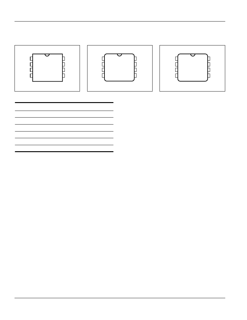
PIN CONFIGURATION
8-Pin DIP
1
2
3
4
8
7
6
5
CS
SK
D
IN
D
OUT
VCC
NC
NC
GND
PIN CONFIGURATION
8-Pin JEDEC Small Outline
“
G
”
PIN CONFIGURATION
8-Pin JEDEC Small Outline
“
GR
”
1
2
3
4
8
7
6
5
NC
VCC
CS
SK
NC
GND
D
OUT
D
IN
1
2
3
4
8
7
6
5
CS
SK
D
IN
D
OUT
VCC
NC
NC
GND
PIN DESCRIPTIONS
CS
Chip Select
SK
Serial Data Clock
D
IN
Serial Data Input
D
OUT
Serial Data Output
NC
Not Connected
Vcc
Power
GND
Ground
Low Voltage Read
The IS93C56-3 has been designed to ensure that data
read operations are reliable in low voltage environments.
The IS93C56-3 is guaranteed to provide accurate data
during read operations with Vcc as low as 2.7V.
Auto Increment Read Operations
In the interest of memory transfer operation applications,
the IS93C56-3 has been designed to output a continuous
stream of memory content in response to a single read
operation instruction. To utilize this function, the system
asserts a read instruction specifying a start location ad-
dress. Once the 16 bits of the addressed word have been
clocked out, the data in consecutively higher address
locations is output. The address will wrap around continu-
ously with CS HIGH until the chip select (CS) control pin is
brought LOW. This allows for single instruction data dumps
to be executed with a minimum of firmware overhead.
Write Enable (WEN)
The write enable (WEN) instruction must be executed
before any device programming (WRITE, WRALL, ERASE,
and ERAL) can be done. When Vcc is applied, this device
ENDURANCE AND DATA RETENTION
The IS93C56-3 is designed for applications requiring up to
100,000
programming cycles
(WRITE, WRALL, ERASE and
ERAL).
It provides 10 years of secure data retention, without
power after the execution of
100,000
programming cycles.
DEVICE OPERATION
The IS93C56-3 is controlled by seven 9-bit instructions.
Instructions are clocked in (serially) on the D
IN
pin. Each
instruction begins with a logical
“
1
”
(the start bit). This is
followed by the opcode (2 bits), the address field (8 bits),
and
data,
if appropriate. The clock signal
(SK)
may be halted at any
time and the IS93C56-3 will
remain in its last state. This
allows
full static flexibility and maximum power conservation.
Read (READ)
The READ instruction is the only instruction that outputs
serial data on the D
OUT
pin. After the read instruction and
address have been decoded, data is transferred from the
selected memory register into a 16-bit serial shift register.
(Please note that one logical
“
0
”
bit precedes the actual
16-bit output data string.) The output on D
OUT
changes
during the low-to-high transitions of SK (see Figure 3).
相關(guān)PDF資料 |
PDF描述 |
|---|---|
| IS93C56-3P | 2,048-BIT SERIAL ELECTRICALLY ERASABLE PROM |
| IS93C56-3PI | 2,048-BIT SERIAL ELECTRICALLY ERASABLE PROM |
| IS93C56-3 | 2,048-Bit Serial EEPROM(2KB串行EEPROM) |
| IS93C56A | 2K-BIT/4K-BIT SERIAL ELECTRICALLY ERASABLE PROM |
| IS93C56A-2GRI | 2K-BIT/4K-BIT SERIAL ELECTRICALLY ERASABLE PROM |
相關(guān)代理商/技術(shù)參數(shù) |
參數(shù)描述 |
|---|---|
| IS93C56-3P | 制造商:ISSI 制造商全稱:Integrated Silicon Solution, Inc 功能描述:2,048-BIT SERIAL ELECTRICALLY ERASABLE PROM |
| IS93C56-3PI | 制造商:ISSI 制造商全稱:Integrated Silicon Solution, Inc 功能描述:2,048-BIT SERIAL ELECTRICALLY ERASABLE PROM |
| IS93C56A | 制造商:ISSI 制造商全稱:Integrated Silicon Solution, Inc 功能描述:2K-BIT/4K-BIT SERIAL ELECTRICALLY ERASABLE PROM |
| IS93C56A-2GRI | 功能描述:電可擦除可編程只讀存儲(chǔ)器 1.8V 2Kb Industrial Temp RoHS:否 制造商:Atmel 存儲(chǔ)容量:2 Kbit 組織:256 B x 8 數(shù)據(jù)保留:100 yr 最大時(shí)鐘頻率:1000 KHz 最大工作電流:6 uA 工作電源電壓:1.7 V to 5.5 V 最大工作溫度:+ 85 C 安裝風(fēng)格:SMD/SMT 封裝 / 箱體:SOIC-8 |
| IS93C56A-2GRI-TR | 功能描述:電可擦除可編程只讀存儲(chǔ)器 1.8V 2Kb Industrial Temp RoHS:否 制造商:Atmel 存儲(chǔ)容量:2 Kbit 組織:256 B x 8 數(shù)據(jù)保留:100 yr 最大時(shí)鐘頻率:1000 KHz 最大工作電流:6 uA 工作電源電壓:1.7 V to 5.5 V 最大工作溫度:+ 85 C 安裝風(fēng)格:SMD/SMT 封裝 / 箱體:SOIC-8 |
發(fā)布緊急采購,3分鐘左右您將得到回復(fù)。