- 您現(xiàn)在的位置:買賣IC網(wǎng) > PDF目錄360914 > IQX320-15PP391I User Programmable Special Function ASIC PDF資料下載
參數(shù)資料
| 型號: | IQX320-15PP391I |
| 英文描述: | User Programmable Special Function ASIC |
| 中文描述: | 用戶可編程ASIC的特殊功能 |
| 文件頁數(shù): | 24/65頁 |
| 文件大?。?/td> | 620K |
| 代理商: | IQX320-15PP391I |
第1頁第2頁第3頁第4頁第5頁第6頁第7頁第8頁第9頁第10頁第11頁第12頁第13頁第14頁第15頁第16頁第17頁第18頁第19頁第20頁第21頁第22頁第23頁當(dāng)前第24頁第25頁第26頁第27頁第28頁第29頁第30頁第31頁第32頁第33頁第34頁第35頁第36頁第37頁第38頁第39頁第40頁第41頁第42頁第43頁第44頁第45頁第46頁第47頁第48頁第49頁第50頁第51頁第52頁第53頁第54頁第55頁第56頁第57頁第58頁第59頁第60頁第61頁第62頁第63頁第64頁第65頁
IQX Family Data Sheet
24
Revision 5.0
June 2000
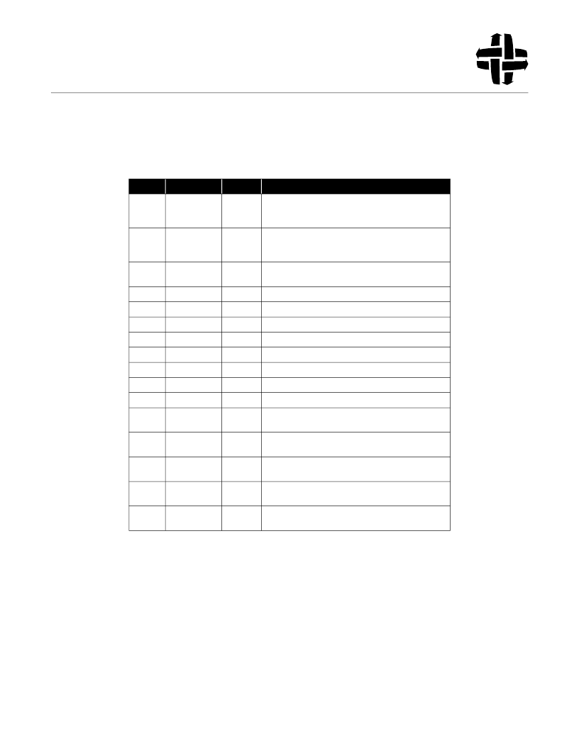
2.4 Mode Control Register
The IQX device contains a 16-bit Mode Control Register. It
stores the RapidConfigure Enable and certain other non-user
flags which must be set correctly for the proper functioning of the
device. Table 10 shows the bit assignment and their function.
A special JTAG instruction is used to write to the Mode Control
Register. When this register is written using JTAG the least
significant bit (Bit 0) is shifted in first.
Bit #
Name
Default
Description
0
KCNT
0
Key Counter Enable.
When set, uses the internal 5-bit counter to provide
Key Address
1
RM
*
Used to enable IOB configuration through
RapidConfigure interface.
Default value equals the RCE pin value on Reset.
2
RC
*
Enables or disables RapidConfigure mode.
Default value equals the RCE pin value on Reset.
3
IOB_PU1
1
IOB Pull Up 10k Ref
4
BRO_PW1
1
BR external one-shot Pulse Width 10k Ref
5
BRI_PW1
1
BR internal one-shot Pulse Width 10k Ref
6
C_PUMP
1
Charge Pump Enable Bit
7
IOB_PU2
0
IOB Pull Up 20k Ref
8
BRO_PW2
0
BR external one-shot Pulse Width 20k Ref
9
BRI_PW2
0
BR internal one-shot Pulse Width 20k Ref
10
INTERNAL
0
For internal use. Should not be changed by the user.
11
KVAL0
0
Terminal count value bit 0 (LSB) when internal
counter is used as Key Address
12
KVAL1
0
Terminal count value bit 1 when internal counter is
used as Key Address
13
KVAL2
0
Terminal count value bit 2 when internal counter is
used as Key Address
14
KVAL3
0
Terminal count value bit 3 when internal counter is
used as Key Address
15
KVAL4
0
Terminal count value bit 4 (MSB) when internal
counter is used as Key Address
Table 10. Mode Control Register Bit Assignment
Powered by ICminer.com Electronic-Library Service CopyRight 2003
相關(guān)PDF資料 |
PDF描述 |
|---|---|
| IQX320-7PP391 | User Programmable Special Function ASIC |
| IQX320-PB416 | User Programmable Special Function ASIC |
| IR00 | ASIC |
| IR01HD224-P2 | PERIPHERAL DRIVER|1 DRIVER|CMOS|SIP|9PIN|PLASTIC |
| IR01HD420 | PERIPHERAL DRIVER|1 DRIVER|CMOS|SIP|9PIN|PLASTIC |
相關(guān)代理商/技術(shù)參數(shù) |
參數(shù)描述 |
|---|---|
| IQXO-22C-24.0 | 制造商:IQD Frequency Products 功能描述:OSCILLATOR CRYSTAL |
| IQXO-22C-32MHZ | 制造商:IQD Frequency Products 功能描述:OSCILLATOR CRYSTAL |
| IQXO-22C-4.0 | 制造商:IQD Frequency Products 功能描述:OSCILLATOR CRYSTAL |
| IQXO-22C-50.0 | 制造商:IQD Frequency Products 功能描述:OSCILLATOR CRYSTAL |
| IQXO-331-100.0MHz | 制造商:IQD Frequency Products 功能描述:CRYSTAL OSCILLATOR 100.000000MHZ |
發(fā)布緊急采購,3分鐘左右您將得到回復(fù)。