- 您現(xiàn)在的位置:買賣IC網(wǎng) > PDF目錄360914 > IQX320-15PP391 User Programmable Special Function ASIC PDF資料下載
參數(shù)資料
| 型號(hào): | IQX320-15PP391 |
| 英文描述: | User Programmable Special Function ASIC |
| 中文描述: | 用戶可編程ASIC的特殊功能 |
| 文件頁(yè)數(shù): | 34/65頁(yè) |
| 文件大?。?/td> | 620K |
| 代理商: | IQX320-15PP391 |
第1頁(yè)第2頁(yè)第3頁(yè)第4頁(yè)第5頁(yè)第6頁(yè)第7頁(yè)第8頁(yè)第9頁(yè)第10頁(yè)第11頁(yè)第12頁(yè)第13頁(yè)第14頁(yè)第15頁(yè)第16頁(yè)第17頁(yè)第18頁(yè)第19頁(yè)第20頁(yè)第21頁(yè)第22頁(yè)第23頁(yè)第24頁(yè)第25頁(yè)第26頁(yè)第27頁(yè)第28頁(yè)第29頁(yè)第30頁(yè)第31頁(yè)第32頁(yè)第33頁(yè)當(dāng)前第34頁(yè)第35頁(yè)第36頁(yè)第37頁(yè)第38頁(yè)第39頁(yè)第40頁(yè)第41頁(yè)第42頁(yè)第43頁(yè)第44頁(yè)第45頁(yè)第46頁(yè)第47頁(yè)第48頁(yè)第49頁(yè)第50頁(yè)第51頁(yè)第52頁(yè)第53頁(yè)第54頁(yè)第55頁(yè)第56頁(yè)第57頁(yè)第58頁(yè)第59頁(yè)第60頁(yè)第61頁(yè)第62頁(yè)第63頁(yè)第64頁(yè)第65頁(yè)
IQX Family Data Sheet
34
Revision 5.0
June 2000
Notes:
(1) These parameters are guaranteed but not tested in production.
(2) The timng parameters are specified for a configuration where an Input Port is driving one Output Port. For configurations where an Input Port is
driving two or more Output Ports, the timng parameters are de-rated as shown in Section 5.7 or Table 20. These parameters are guaranteed but
not tested in production.
t
KW-RO
t
KS-RO
t
KH-RO
t
KCO-RO
t
KPZH-IT
t
KPZL-IT
t
KPZH-OT
t
KPZL-OT
t
KPHZ-OT
t
KPLZ-OT
t
KW-LI
t
KS-LI
t
KH-LI
t
KCO-LI
t
KP-LIT
t
KW-LO
t
KS-LO
t
KH-LO
t
KCO-LO
t
KP-LOT
f
KCNT
t
WKCNT
t
S_KCKE
t
H_KCKE
t
S_KRST
t
H_KRST
t
KCLK_OE
t
KCLK_IE
t
P_KCLR
t
P_KF1F
T
RC
t
W+ -RC
, t
W- -RC
t
S-RC
t
H-RC
t
P-RC
f
JTAG
t
W-JTAG
t
S-JTAG
t
H-JTAG
t
P-JTAG
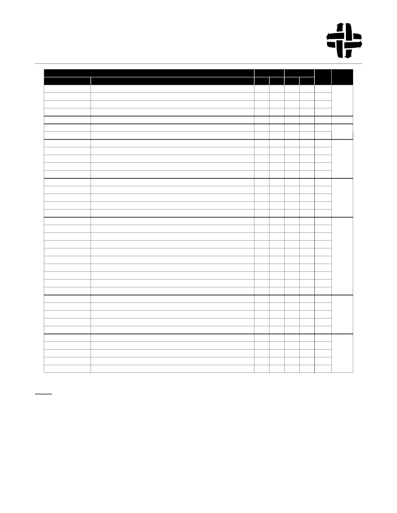
Register Output, MinimumPulse Width of KEY as Clock Enable, Low or High
Register Output, Clock Enable (Key) Setup Time to CLK (GC)
Register Output, CLK (GC) to Clock Enable (Key) Hold Time
Register Output, Key Clock to Output Data Valid
Input Enable (Key) to Data Valid
Output Enable (Key) to Data Valid
Output Enable (Key) to Output at High Z
(1)
Latch Input, MinimumPulse Width of KEY as Latch Enable, Low or High
Latch Input, Data Setup Time to Latch Enable (Key) Trailing Edge
Latch Input, Data to Latch Enable (Key) Trailing Edge Hold Time
Latch Input, Latch Enable (Key) Leading Edge to Data Out
Latch Input, Transparent Mode Propagation Delay
Latch Output, MinimumPulse Width of KEY as Latch Enable, Low or High
Latch Output, Data Setup Time to Latch Enable (Key) Trailing Edge
Latch Output, Data to Latch Enable (Key) Trailing Edge Hold Time
Latch Output, Latch Enable (Key) Leading Edge to Data Out
Latch Output, Transparent Mode Propagation Delay
Key Counter, Input Clock Frequency
Key Counter Clock, Pulse Width
Key Counter, Enable Setup Time to KCLK
Key Counter, KCLK to Enable Hold Time
Key Counter, Reset Setup Time to KCLK
Key Counter, KCLK to Reset Hold Time
Key Counter, Clock to Output Data Valid or Output High Z
Key Counter, Clock to Input Data Valid
Key Counter, Clear to Output Active / High Z Delay
Key Counter, Force 0x1F to Output Active / High Z Delay
RapidConfigure Strobe Period
RapidConfigure Strobe Pulse Width
RapidConfigure Address and Data Setup Time to Strobe
RapidConfigure Address and Data Hold Time to Strobe
RapidConfigure Strobe Falling Edge to Data Valid (Make Connection)
JTAG Clock (TCK) Frequency
JTAG Clock (TCK) Pulse Width
JTAG Setup Time
JTAG Hold Time
JTAG Clock to Output Data Valid
5.0
4.5
0.0
6.0
5.0
0.0
ns
ns
ns
ns
ns
ns
ns
ns
ns
ns
ns
ns
ns
ns
ns
ns
ns
MHz
ns
ns
ns
ns
ns
ns
ns
ns
ns
ns
ns
ns
ns
ns
MHz
ns
ns
ns
ns
22
6.5
9.0
7.5
7.5
7.5
11.0
9.0
9.0
23
24
5.0
2.5
2.0
6.0
3.0
2.0
25
10.5
7.5
13.0
10.0
5.0
4.5
0.0
6.0
5.0
0.0
26
6.5
7.5
80
7.5
10.0
66
5.0
2.0
0.0
2.0
0.0
6.0
2.5
0.0
2.5
0.0
27
8.0
9.5
9.5
8.5
9.5
11.5
11.5
10.5
15.0
6.0
2.0
0.0
17.0
7.5
3.0
0.0
28
25.0
10
30.0
10
20.0
4.0
0.0
15.0
20.0
4.0
0.0
15.0
29
Speed Grade
-7
-10
Units
Ref.
Figure
Symbol
Parameter
Min
Max
Min
Max
Table 19. AC Electrical Specifications for IQX160 and IQX128B (Continued)
Powered by ICminer.com Electronic-Library Service CopyRight 2003
相關(guān)PDF資料 |
PDF描述 |
|---|---|
| IQX320-15PP391I | User Programmable Special Function ASIC |
| IQX320-7PP391 | User Programmable Special Function ASIC |
| IQX320-PB416 | User Programmable Special Function ASIC |
| IR00 | ASIC |
| IR01HD224-P2 | PERIPHERAL DRIVER|1 DRIVER|CMOS|SIP|9PIN|PLASTIC |
相關(guān)代理商/技術(shù)參數(shù) |
參數(shù)描述 |
|---|---|
| IQXO-22C-24.0 | 制造商:IQD Frequency Products 功能描述:OSCILLATOR CRYSTAL |
| IQXO-22C-32MHZ | 制造商:IQD Frequency Products 功能描述:OSCILLATOR CRYSTAL |
| IQXO-22C-4.0 | 制造商:IQD Frequency Products 功能描述:OSCILLATOR CRYSTAL |
| IQXO-22C-50.0 | 制造商:IQD Frequency Products 功能描述:OSCILLATOR CRYSTAL |
| IQXO-331-100.0MHz | 制造商:IQD Frequency Products 功能描述:CRYSTAL OSCILLATOR 100.000000MHZ |
發(fā)布緊急采購(gòu),3分鐘左右您將得到回復(fù)。